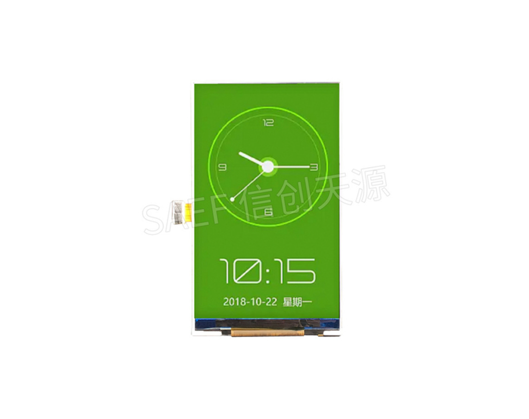
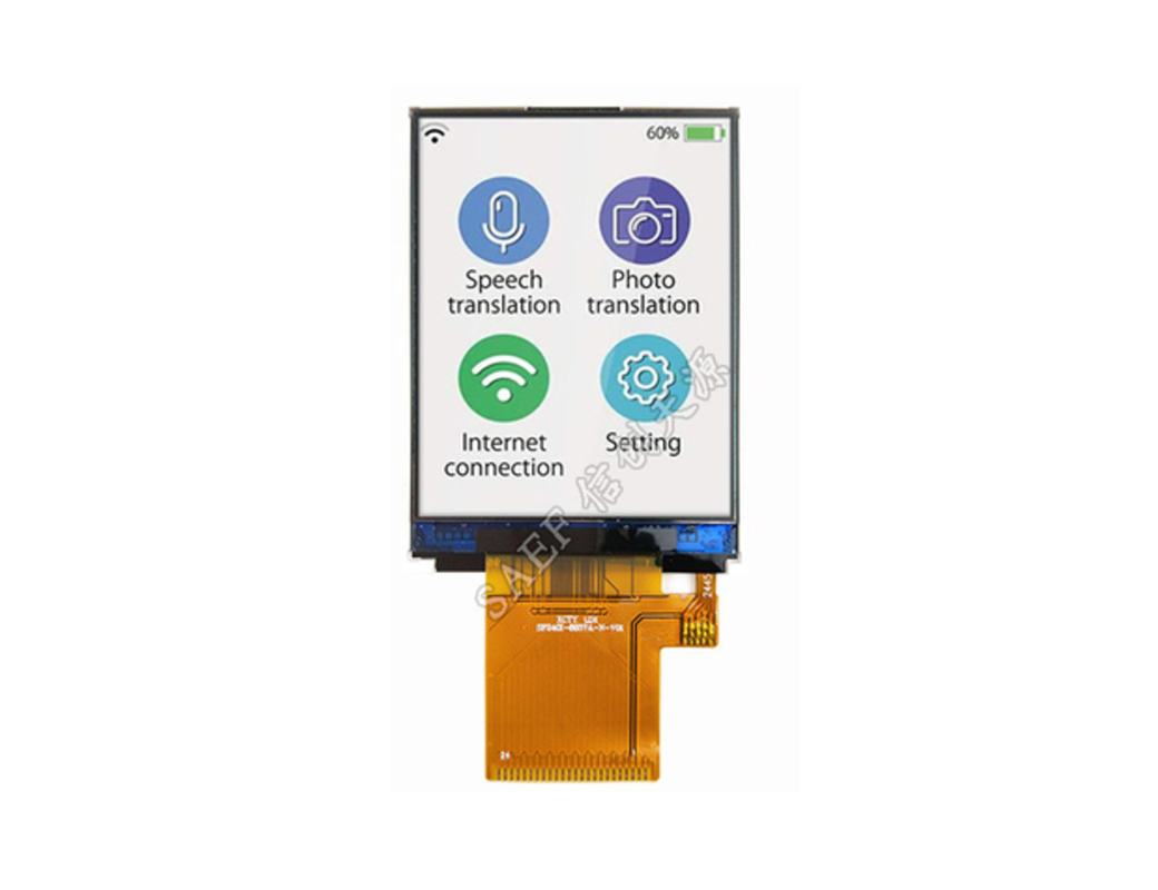
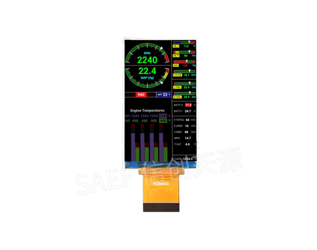
TFT彩屏
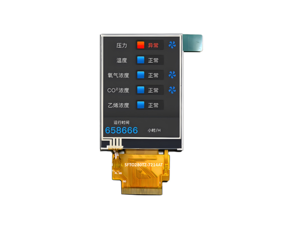
TFT触摸屏
HDMI TFT显示器
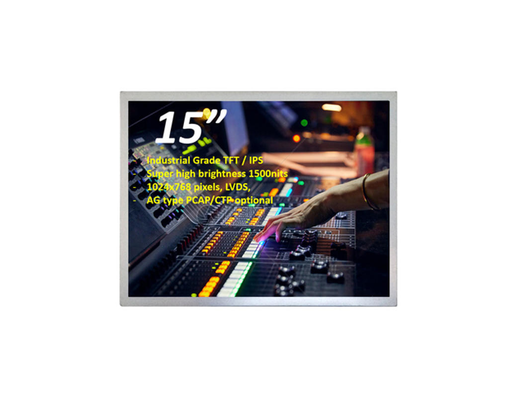
工业级TFT屏
条型TFT屏
圆形TFT屏
方形TFT屏
全视角TFT屏
电阻触摸TFT屏
电子墨水屏
高亮液晶屏
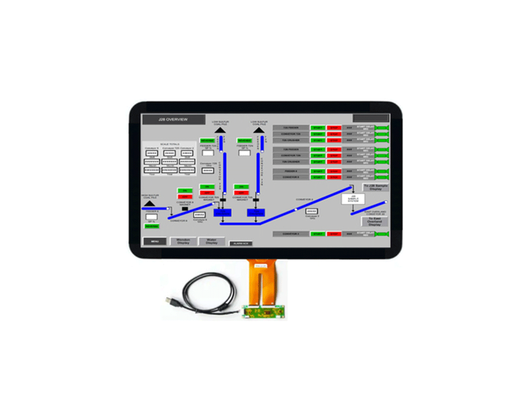
树莓派触摸屏
OLED模块
TFT彩屏
TFT触摸屏
HDMI TFT显示器
工业级TFT屏
条型TFT屏
圆形TFT屏
方形TFT屏
全视角TFT屏
电阻触摸TFT屏
电子墨水屏
高亮液晶屏
树莓派触摸屏
OLED模块

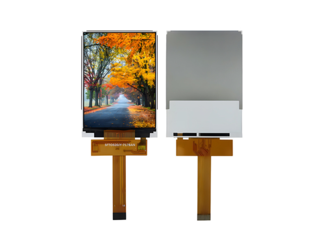
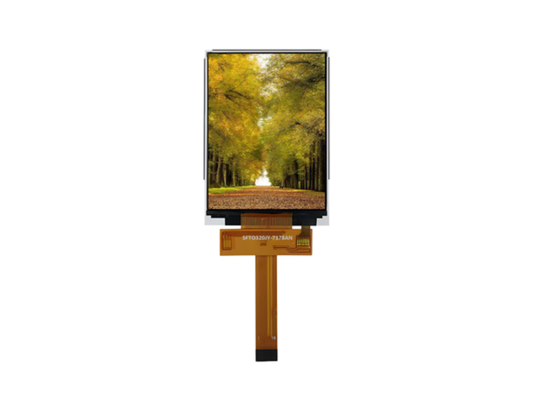
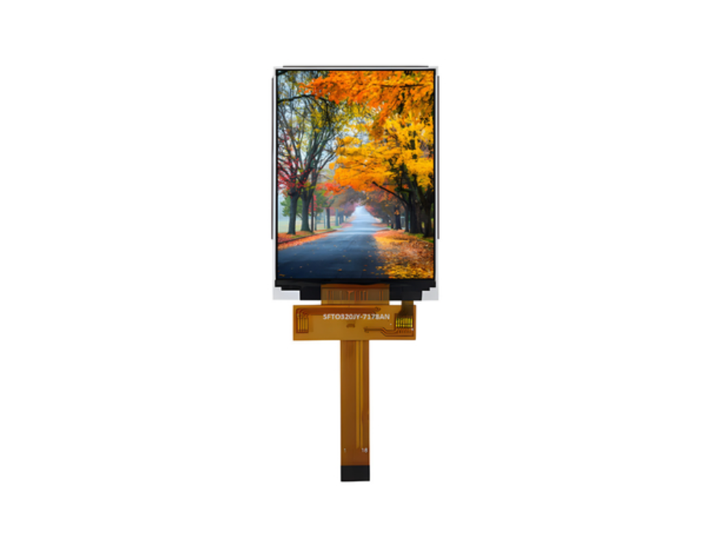
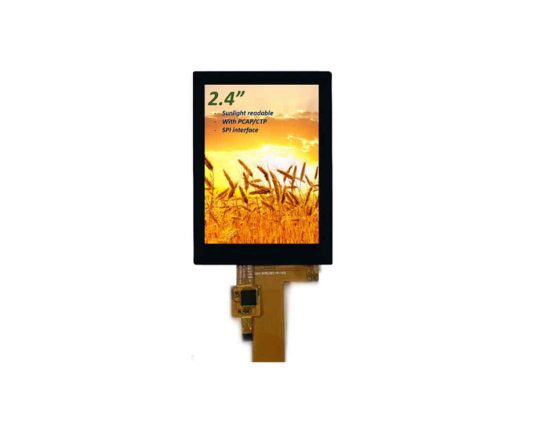
| Product: | 3.2" Inch TFT LCD Display | Resolution: | 240x320 |
| Viewing Direction: | 12 O'clock | Interface: | 4-line SPI |
| Outline Dimension: | 54.0(W)x77.4(H)x2.4(T)(mm) | Active Area: | 48.60(W)x64.80 (H) (mm) |
| Pin Number: | 18 Pins | Connection: | FPC Plugging |
| Surface Luminance: | 350 Cd/m2 (nits) | LED Lifetime: | 40,000 Hours |
| Certificate: | ISO9001:2015 / ISO1400:2015 | Compliance: | Rohs & Reach Compliant |
| Highlight: | 3.2 Inch SPI TFT LCD Display, 18 Pin TFT LCD Display, 240*320 Pixels TFT LCD Display | ||
产品介绍
3.2英寸SPI TFT显示屏是彩色TFT液晶显示屏,具有240 x 320点阵SPI接口,具有丰富的色彩显示和高分辨率,为用户提供清晰的视觉体验。适用于工业设备、手持检测仪器、美容设备、智能家居、消费电子等多种应用场景。
这款3.2寸SPI TFT SFTO320JY-7178AN模块内置ST7789V驱动IC;它支持 4 线 SPI 接口,电源电压 (VDD) 范围为 2.8V 至 3.3V。工作温度范围为-20℃至+70℃,存储温度范围为-30℃至+80℃。
基于这款3.2英寸SPI TFT产品,赛尔科技提供差异化的定制解决方案,包括但不限于:
背光定制:根据产品需求调整背光类型和亮度。
接口定制:改变液晶屏排线的结构和接口,以适应特定的硬件平台。
触摸屏集成:可选电阻式或电容式触摸屏,增强用户交互体验。
特征
| Product: | 3.2" Inch TFT LCD Display |
| Model number | SFTO320JY-7178AN |
| Resolution: | 240x320 |
| Viewing Direction: | 12 O'clock |
| Interface: | 4-line SPI |
| Outline Dimension: | 54.0(W)x77.4(H)x2.4(T)(mm) |
| Active Area: | 48.60(W)x64.80 (H) (mm) |
| Pin Number: | 18 Pins |
| Connection: | FPC Plugging |
| Surface Luminance: | 350 Cd/m2 (nits) |
| LED Lifetime: | 40,000 Hours |
| Certificate: | ISO9001:2015 / ISO1400:2015 |
| Compliance: | Rohs & Reach Compliant |
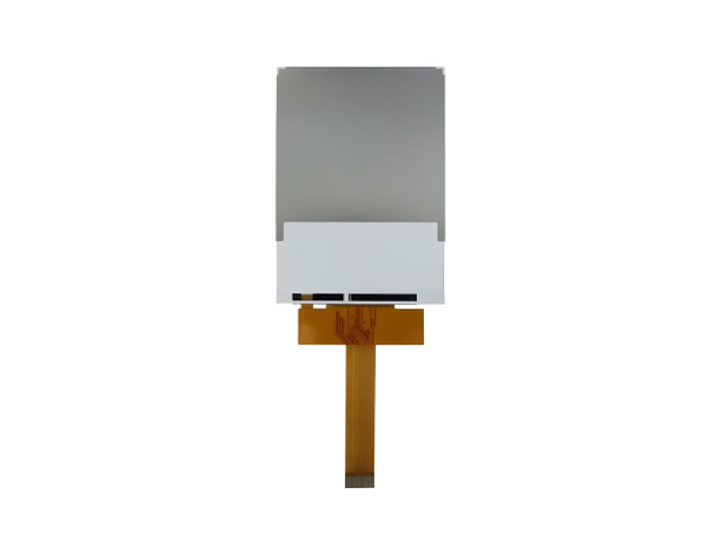
外形图


电气最大额定值
| Item | Symbol | Min | Max | Unit | Note |
| Supply voltage(VDDI) | V | 1.8 | 3.3 | V | - |
| Supply voltage(VDD) | V | 2.8 | 3.3 | V | - |
| Operating temperature | TOPR | -20 | 70 | ℃ | - |
| Storage temperature | TSTR | -30 | 80 | ℃ | - |
背光特性
| Item | Symbol | Min | Typical | Max | Unit |
| LED module Forward voltage | VLED | 2.9 | 3.1 | 3.3 | V |
| LED module current | ILED | - | 90 | - | mA |
| LCD Surface Luminance | LS | 330 | 350 | - | Cd/m2 |
| LCM Surface brightness uniform | LD | 80 | - | - | % |
| LCD power dissipation | PLCD | - | 0.32 | - | W |
接口引脚定义
| PIN No. | Symbol | Description |
| 1 | GND | Ground |
| 2 | RESET | -This signal will reset the device and it must be applied to properly initialize the chip. -Signal is active low. |
| 3 | SCL | -This pin is used to be serial interface clock. |
| 4 | D/C | - Display data/command selection pin in 4-line serial interface. |
| 5 | CSX | -Chip selection pin, Low enable. High disable. |
| 6 | SDA | SPI interface input pin. -The data is latched on the rising edge of the SCL signal. -If not used, please fix this pin at VDDI or DGND level. |
| 7 | SDO | -SPI interface output pin. -The data is output on the falling edge of the SCL signal. -If not used, let this pin open. |
| 8 | GND | Ground |
| 9 | VDD | Power Supply for Analog, Digital System and Booster Circuit. |
| 10 | LEDA | Anode of Backlight (2.9V-3.3V Typical:3.1V) |
| 11 | LEDK | Cathode of Backlight |
| 12 | LEDK | Cathode of Backlight |
| 13 | LEDK | Cathode of Backlight |
| 14 | LEDK | Cathode of Backlight |
| 15 | XL | Touch panel Logical foot |
| 16 | YU | Touch panel Logical foot |
| 17 | XR | Touch panel Logical foot |
| 18 | YD | Touch panel Logical foot |
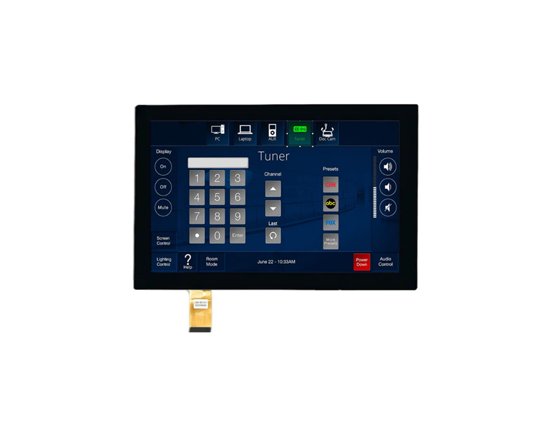
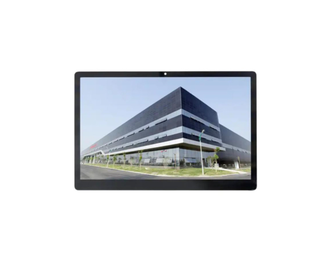
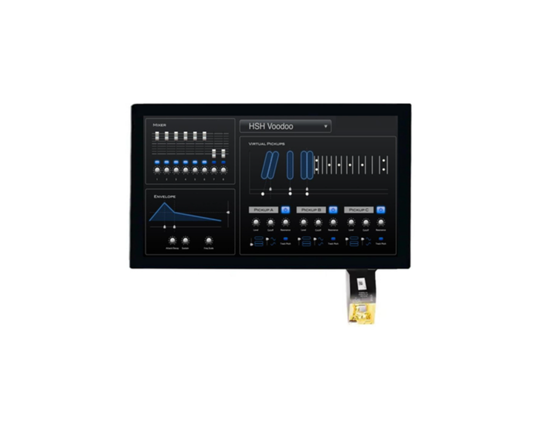
产品图片


设施和认证


手机/微信:135 0298 3321 柯先生
手机/微信:138 2960 7086 郑小姐
手机/微信:136 8686 7235 陈小姐
地址: 深圳市宝安区洲石路阳光工业区D栋


在线留言

 135 0298 3321
 首页 》
首页 》