TFT彩屏
TFT触摸屏
HDMI TFT显示器
工业级TFT屏
条型TFT屏
圆形TFT屏
方形TFT屏
全视角TFT屏
电阻触摸TFT屏
电子墨水屏
高亮液晶屏
树莓派触摸屏
OLED模块
TFT彩屏
TFT触摸屏
HDMI TFT显示器
工业级TFT屏
条型TFT屏
圆形TFT屏
方形TFT屏
全视角TFT屏
电阻触摸TFT屏
电子墨水屏
高亮液晶屏
树莓派触摸屏
OLED模块

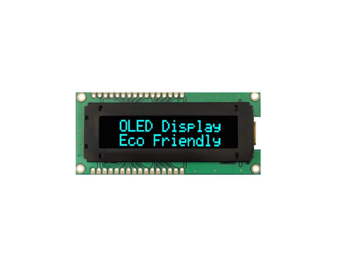
| Product: | 0.96" OLED Display | Number Of Pixels: | 128x64 Pixels |
| Driver IC: | SSD1315 Or Equivalent | Display Mode: | Passive Matrix |
| Display Color: | Monochrome (white) | Drive Duty: | 1/64 Duty |
| Panel Size: | 24.7 X 16.6 X 1.3 (mm) | Active Area: | 21.74 X 11.175 (mm) |
| Viewing Direction: | All Viewing Angles | Interface: | SPI/I2C/8080 |
| Connection: | Plug-in | Pin Number: | 30 Pins (Can Be Customized) |
| Operating Temp.: | -40C - +70C | Storage Temp.: | -40C - +85C |
| Life Time: | 50,000 Hours @60cd/m2 | Compliance: | REACH & RoHS Compliant |
| Highlight: | 128X64 OLED Display, SPI OLED Display, 30 Pins OLED Display | ||
批发价0.96英寸OLED显示屏产品介绍
0.96英寸OLED显示屏是一种小型自发光显示器件,由于其轻薄、低功耗、高对比度、宽视角等特点,广泛应用于各种智能设备和仪器中。 0.96英寸OLED显示屏通常采用SSD1315/SSD1306驱动芯片,支持多种接口模式,包括6800和8080并行、3线或4线串行SPI以及IIC接口模式。这类显示屏具有自发光特性,不需要背光源,因而显示性能更好、响应速度更快、可视角度更宽。
SAEF TECHNOLOGY生产的0.96英寸OLED显示屏广泛应用于智能手机、智能手表、健康监测设备、工业控制系统、便携式游戏机以及其他需要小型高效显示屏的场合。随着技术的不断进步和市场需求的增长,SAEF TECHNOLOGY的0.96英寸OLED显示屏有望在显示性能、能源效率和成本效益方面得到进一步优化和提高。同时,随着物联网和可穿戴设备的快速发展,这种小型OLED显示器的应用前景将更加广阔。
在规模化生产的支撑下,SAEF TECHNOLOGY控制生产成本,优化生产工艺,使得0.96英寸小尺寸OLED产品成本极低,满足了大量用户量产的需求。
特征
| Items | Specification | Unit |
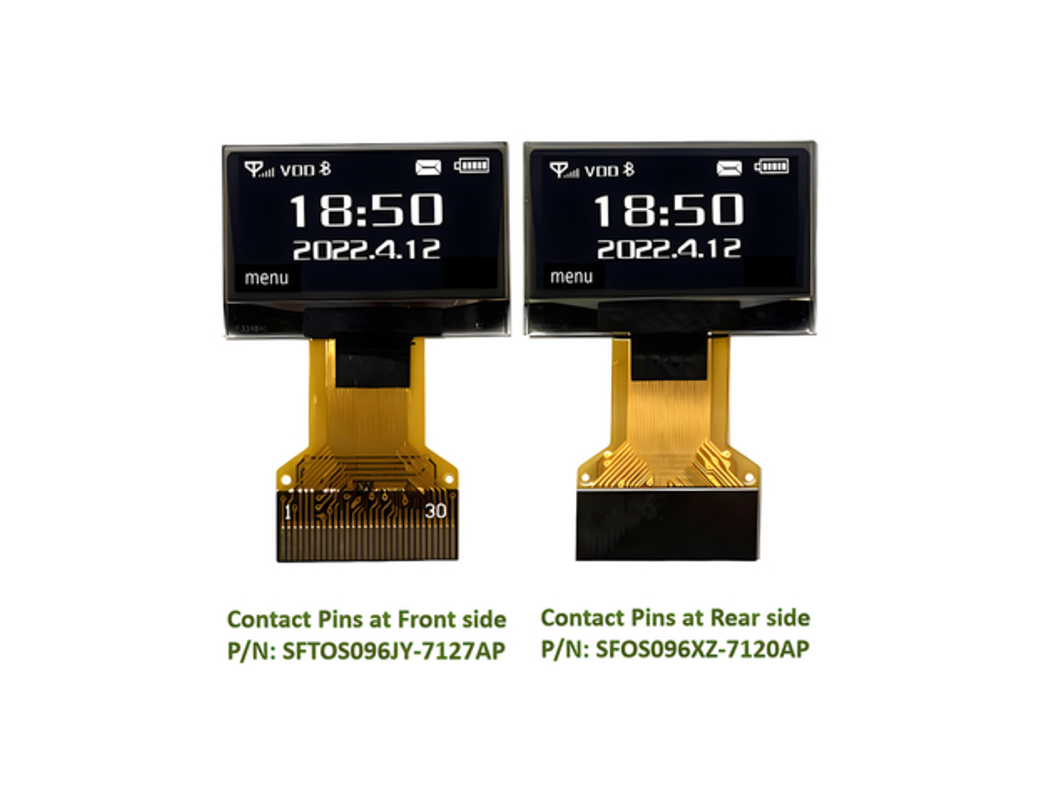
| Model No. | SFOS096XZ-7120AP | |
| Diagonal Size | 0.96 | Inch |
| Resolution | 128x 64 | Dots |
| Active Area | 21.740(W) x 11.175(H) | mm2 |
| Outline Dimension | 24.70(W) x 16.60(H) | mm2 |
| Pixel Pitch | 0.170(W) x 0.175(H) | mm2 |
| Pixel Size | 0.150(W) x 0.150(H) | mm2 |
| Driver IC | SSD1315Z | - |
| Display Color | White | - |
| Gray Scale | 1 | Bit |
| Interface | 4-SPI/I2C/8080 | - |
| IC Package Type | COG | - |
| Module Connecting Type | SOLDER | - |
| Thickness | 1.30 ±0.1 | mm |
| Weight | TBD±10% | g |
| Duty | 1/64 | - |
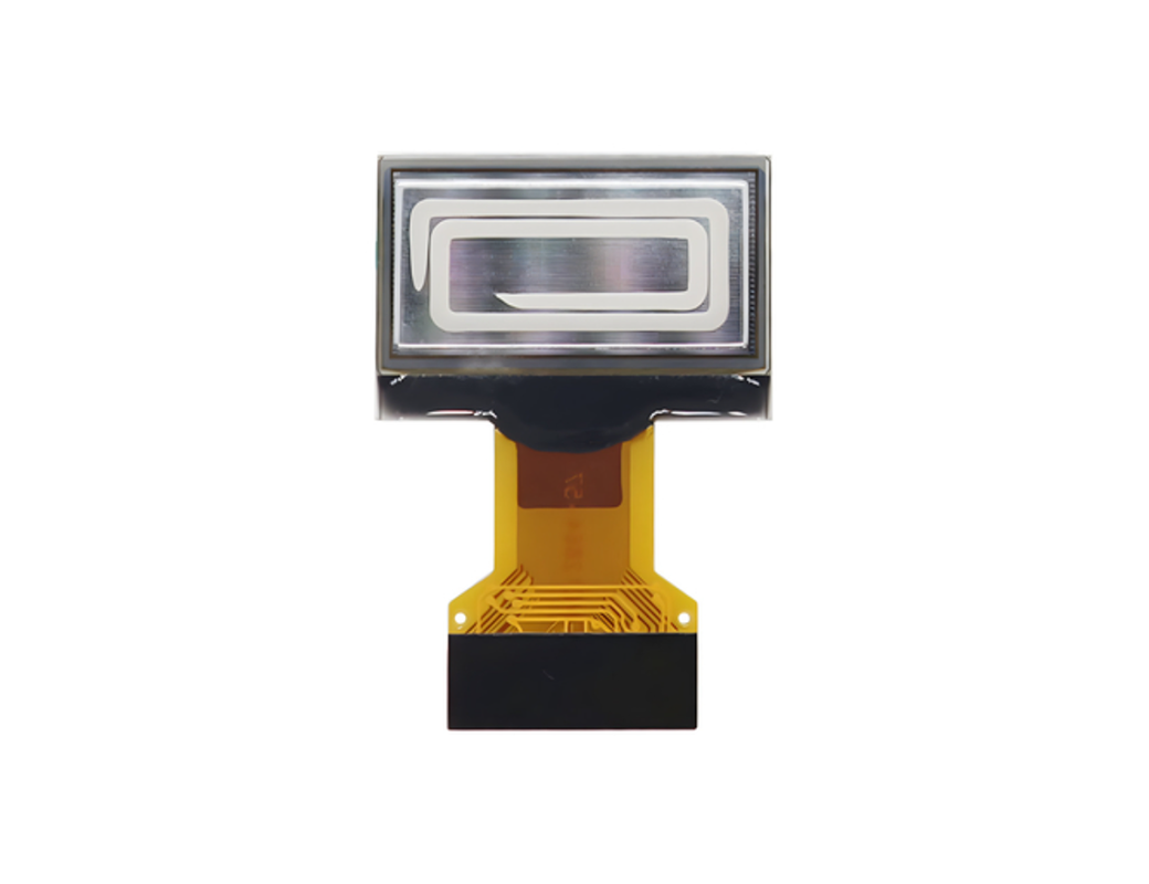
外形图

接口引脚定义
| No | Symbol | Description |
| 1 | NC | No connection. |
| 2 | C1N | CXP/CXN-Pin for charge pump capacitor;Connect to each other with a capacitor |
| 3 | C1P | |
| 4 | C2P | |
| 5 | C2N | |
| 6 | VBAT | Power supply for charge pump regulator circuit. |
| 7,10 | NC | No connection |
| 8 | VSS | This is a ground pin |
| 9 | VDD | Power supply pin for core logic operation. |
| 11 | BS1 | MCU bus interface selection pins. |
| 12 | BS2 | |
| 13 | CS | This is the chip select input.(active LOW) |
| 14 | RES | Reset signal input.when the pin is pulled LOW,initialization of the chip is excute. Keep this pin HIGH(i.e connect to VDD)during normal operation |
| 15 | A0 | This is Data/Command control pin. When it is pulled HIGH (i.e. connect to VDD), the data at D[7:0] is treated as data. |
| When it is pulled LOW, the data at D[7:0] will be transferred to the command register. | ||
| In I2C mode, this pin acts as SA0 for slave address selection. | ||
| When 3-wire serial interface is selected, this pin must be connected to VSS. | ||
| 16 | WR | This is read / write control input pin connecting to the MCU interface. |
| When 8080 interface mode is selected, this pin will be the Write (WR#) input. Data write operation is initiated when this pin is pulled LOW and the chip is selected. | ||
| 17 | RD | When connecting to an 8080-series microprocessor, this pin receives the Read (RD#) signal. Readoperation is initiated when this pin is pulled LOW and the chip is selected. |
| When serial or I2C interface is selected, this pin must be connected to VSS. | ||
| 18 ~25 | D0 | These are 8-bit bi-directional data bus to be connected to the microprocessor鈥檚 data bus. When serial interface mode is selected, D0 will be the serial clock input: SCLK; D1 will be the serialdata input: SDIN and D2 should be kept NC. When I2C mode is selected, D2, D1 should be tied together and serve as SDAout, SDAin in application and D0 is the serial clock input, SCL. |
| ~D7 | ||
| 26 | IREF | This is segment output current reference pin. |
| When external IREF is used, a resistor should be connected between this pin and VSS to maintain the IREF current at 30uA. | ||
| When internal IREF is used, this pin should be kept NC. | ||
| 27 | VCOMH | The pin for COM signal deselected voltage level. |
| A capacitor should be connected between this pin and VSS.Com | ||
| 28 | VCC | Power supply for panel driving voltage. This is also the most positive power voltage supply pin.When charge pump is enabled, a capacitor should be connected between this pin and VSS. |
| 29,30 | NC | No connection |
绝对最大额定值
| Items | Min. | Max. | Unit |
| Supply Voltage(VDD) | -0.3 | +4.0 | V |
| Supply Voltage(VBAT) | -0.3 | +6.0 | V |
| Supply Voltage(VCC) | 0 | +18.0 | V |
| Operating Temperature(TOP) | -40 | 70 | ℃ |
| Storage Temperature(TST) | -40 | 85 | ℃ |
直流特性
| Items | Symbol | Min. | Typ. | Max. | Unit | |
| Supply Voltage | Logic Supply Voltage IC | VDD | 1.65 | 3 | 3.5 | V |
| Charge Pump Regulator Supply VoltageIC | VBAT | 3 | 3.3 | 4.5 | V | |
| Operating(for OLED panel) | VCC | 7 | 7.5 | 8 | V | |
| Input | High Voltage | VIH | 0.8 x VDD | - | VDD | V |
| Voltage | Low Voltage | VIL | 0 | - | 0.2 x VDD | V |
| Output | High Voltage | VOH | 0.9 x VDD | - | VDD | V |
| Voltage | Low Voltage | VOL | VSS | - | 0.1 x VDD | V |
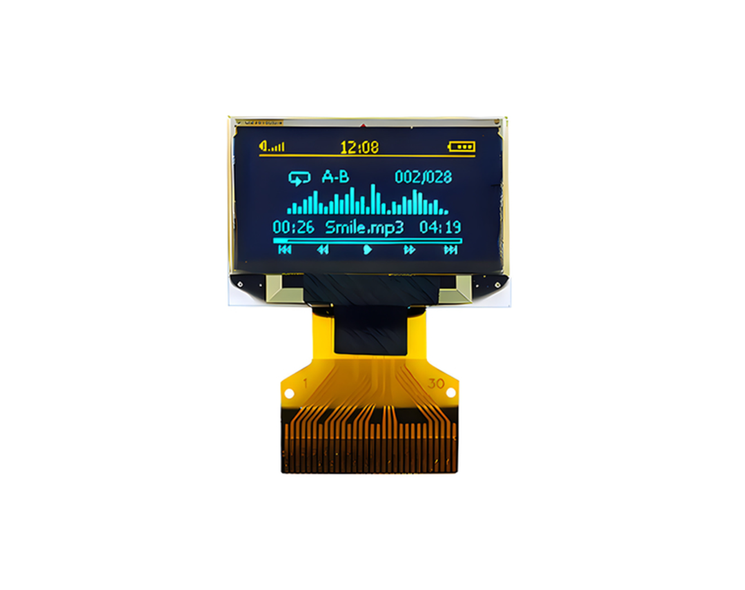
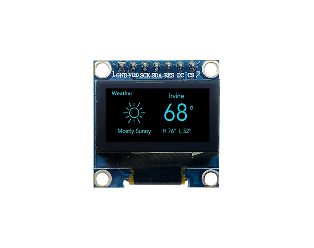
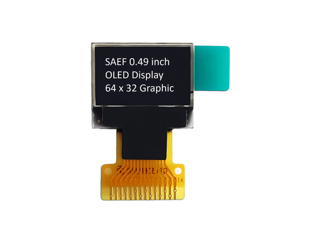
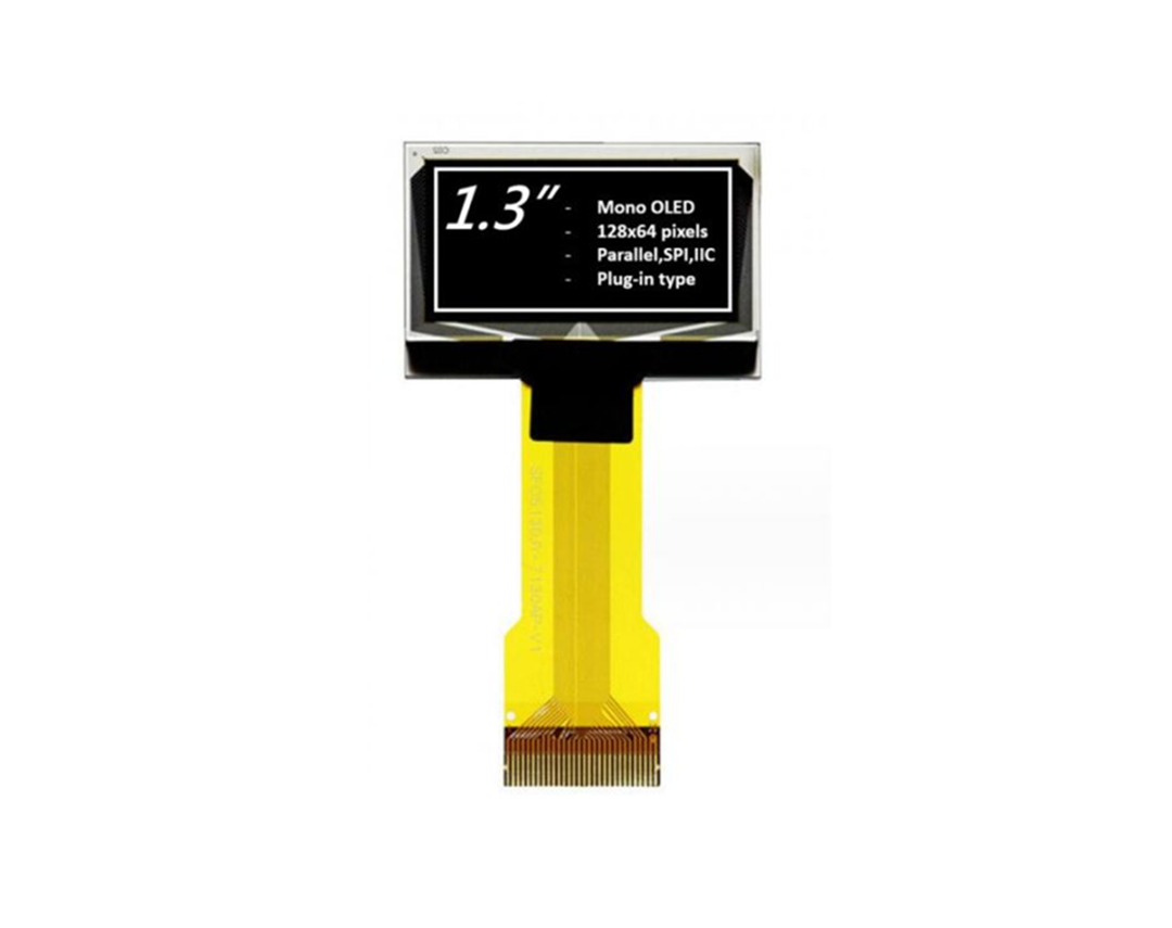
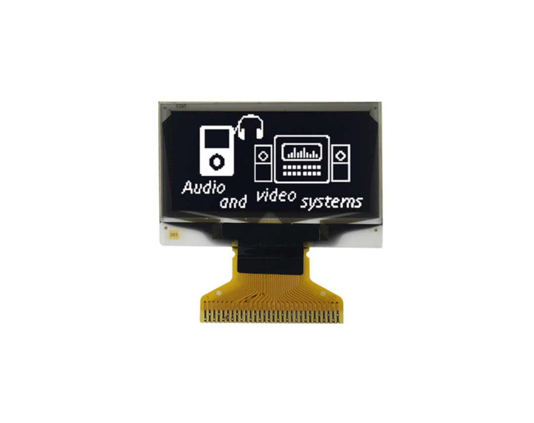
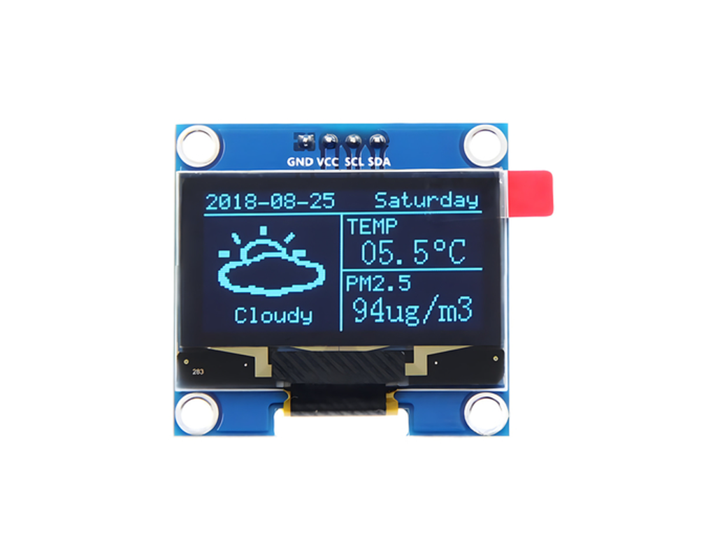
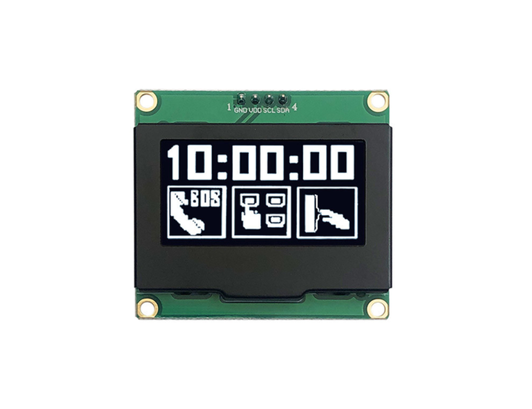
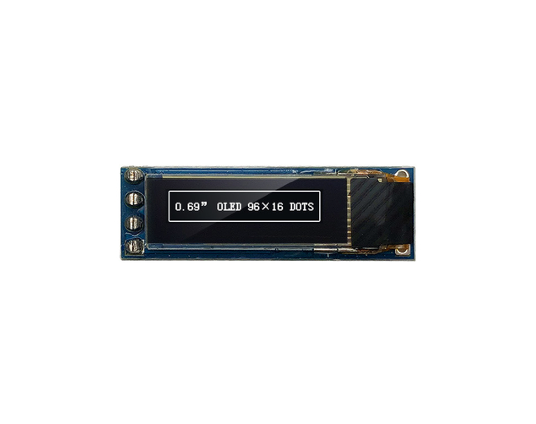
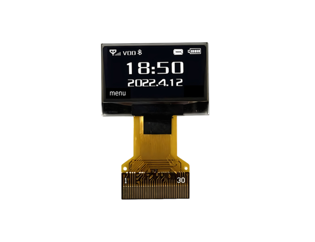
产品图片


可靠性测试
| No. | Item | Condition | Quantity |
| 1 | High Temperature Storage(HTS) | 85±2℃, 200 hours | 3 |
| 2 | High Temperature Operating(HTO) | 70±2℃, 96 hours | 3 |
| 3 | Low Temperature Storage(LTS) | -40±2℃, 200 hours | 3 |
| 4 | Low Temperature Operating(LTO) | -40±2℃, 96 hours | 3 |
| 5 | High Temperature /High Humidity Storage(HTHHS) | 50±3℃, 90%±3%RH, 120 hours | 3 |
| 6 | Thermal Shock (Non-operation)(TS) | -20±2℃ ~ 25℃ ~ 70±2℃ (30min) (5min) (30min) 10cycles | 3 |
| 7 | Vibration (Packing) | 10~55~ 10Hz,amplitude 1.5mm, 1 hour for each direction x, y, z | 1 Carton |
| 8 | Drop (Packing) | Height : 1 m, each time for 6 sides, 3 edges, 1 angle | 1 Carton |
| 9 | ESD (finished product housing) | ±4kVR:330Ω; C:150pF 10times,air discharge | 3 |
设施及证书


手机/微信:135 0298 3321 柯先生
手机/微信:138 2960 7086 郑小姐
手机/微信:136 8686 7235 陈小姐
地址: 深圳市宝安区洲石路阳光工业区D栋


在线留言

 135 0298 3321
 首页 》
首页 》