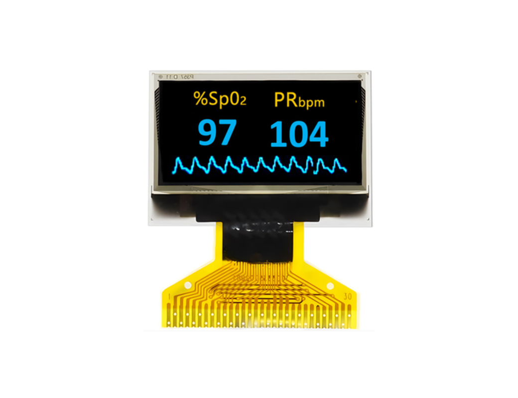
TFT彩屏
TFT触摸屏
HDMI TFT显示器
工业级TFT屏
条型TFT屏
圆形TFT屏
方形TFT屏
全视角TFT屏
电阻触摸TFT屏
电子墨水屏
高亮液晶屏
树莓派触摸屏
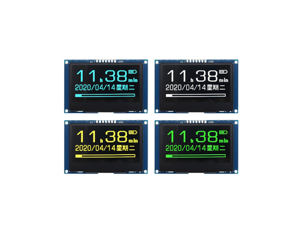
OLED模块
TFT彩屏
TFT触摸屏
HDMI TFT显示器
工业级TFT屏
条型TFT屏
圆形TFT屏
方形TFT屏
全视角TFT屏
电阻触摸TFT屏
电子墨水屏
高亮液晶屏
树莓派触摸屏
OLED模块

| Product: | 1.12 Inch OLED Display Module | Number Of Pixels: | 128x128 Dots |
| Driver IC: | SH1107 Or Equivalent | Display Mode: | Passive Matrix |
| Display Color: | Mono White | Drive Duty: | 1/128 Duty |
| Panel Size: | 27 X 30.1 X 1.25 (mm) | Active Area: | 20.14 X 20.14 (mm) |
| Pixel Pitch: | 0.1575 X 0.1575(mm) | Pixel Size: | 0.1375 X 0.1375(mm) |
| Viewing Direction: | All Viewing Angles | Interface: | 8-bit 68XX/80XX Parallel, 4-wire SPI, I2C |
| Connection: | ZIF | Pin Number: | 20 Pins |
| Life Time: | 50,000 Hours @60cd/m2 | Compliance: | REACH & RoHS Compliant |
| Highlight: | 128x128 Dots OLED Display Module, 1.12 Inch OLED Display Module, SPI I2C Graphic OLED Display | ||
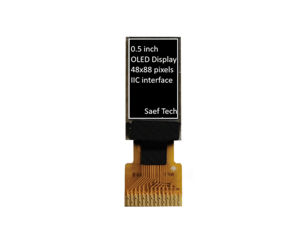
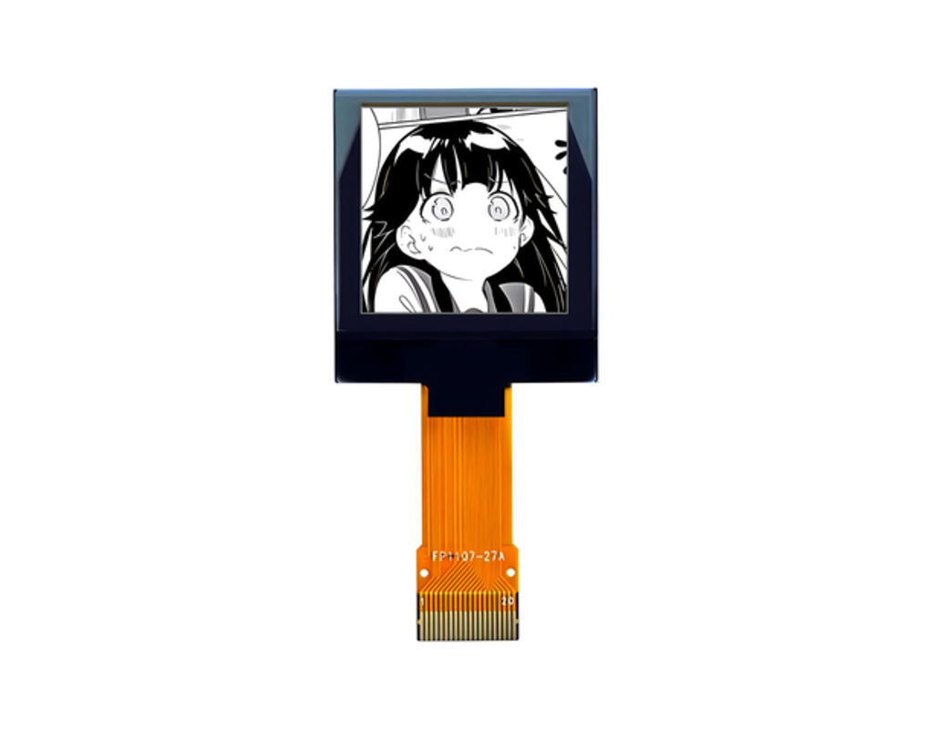
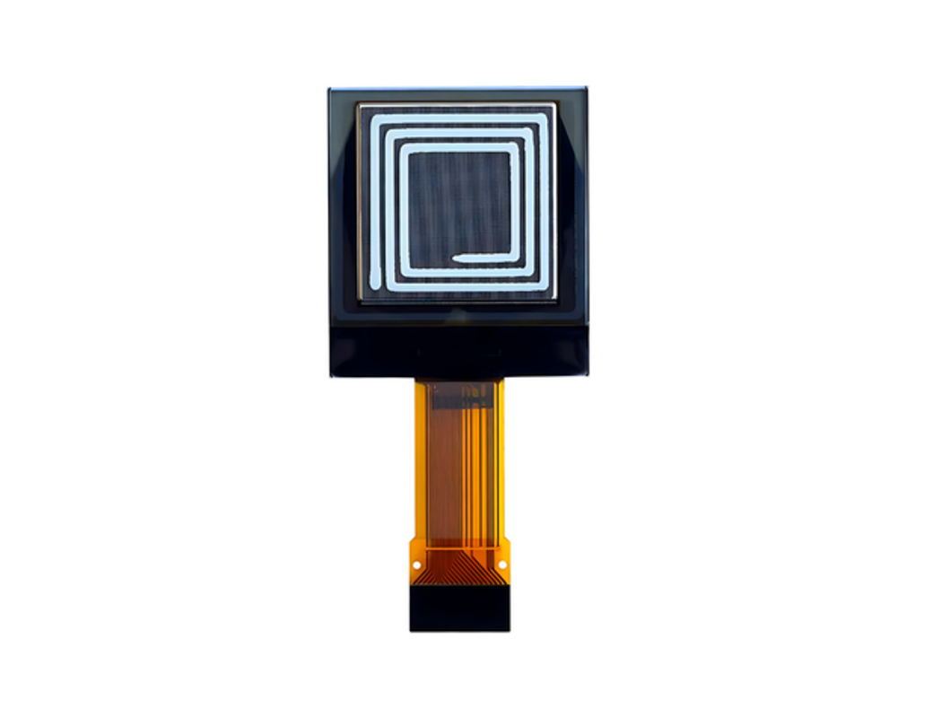
40mm ZIF FPC 1.12英寸OLED显示屏产品介绍
产品快速浏览
· 型号 SFOS112XZ-128128PAN
· 1.12英寸迷你OLED显示屏
· 128X128点分辨率
· SH1107芯片组
· ZIF型连接40mm长度
· 接口:8位68XX/80XX、4线SPI、I2C
· 工作温度:-40℃至+70℃
· 储存温度:-40℃至+80℃
描述
SFOS112XZ-128128PAN OLED 显示模块是一款 128x128 分辨率 COG 图形显示屏,对角线尺寸 1.12 英寸。 OLED型号设计为工业级,具有价格竞争优势。模块内置SH1107 IC;它支持8位68XX/80XX并行、4线SPI、I2C接口。逻辑供电电压为2.8V,显示供电电压为12V,VDD工作电流为55μA,SFOS112XZ-128128PAN OEL显示模块可在-40℃至+70℃温度下工作;其储存温度范围为-40℃至+80℃。
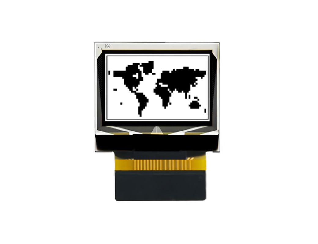
40mm ZIF FPC 1.12英寸OLED显示屏产品图

引脚定义
| Pin Number | Symbol | I/O | Function |
| PowerSuply | |||
| 1 | VPP | P | Power Supplly for OEL Panell This is the most positive voltage supply pin of the chip. It must be supplied externally. |
| 3 | VDD | P | Power Supplly for Logiic This is a voltage supply pin. It must be connected to external source. |
| 20 | GND | P | Ground of OEL System This is a ground pin. It also acts as a reference for the logic pins, the OEL driving voltages, and the analog circuits. It must be connected to external ground. |
| Driver | |||
| 6 | IREF | I | Current Reference for Brightness Adjustment This pin is segment current reference pin. A resistor should be connected between this pin and VSS. Set the current at 12.5μA maximum. |
| 2 | VCOMH | O | Voltage Output High Level for COM Signal This pin is the input pin for the voltage output high level for COM signals. A capacitor should be connected between this pin and VSS. |
| Interface | |||
| 4,5 | BS1 BS2 | I | Communiicatiing Protocoll Sellect These pins are MCU interface selection input. See the following table:
|
| 8 | RES# | I | Power Reset for Controller and Driver This pin is reset signal input. When the pin is low, initialization of the chip is executed. Keep this pin pull high during normal operation. |
| 7 | CS# | I | Chip Select This pin is the chip select input. The chip is enabled for MCU communication only when CS# is pulled low. |
| 9 | A0 | I | Data/Command Controll This pin is Data/Command control pin. When the pin is pulled high, the input at D7~D0 will be interpreted as display data. When the pin is pulled low, the input at D7~D0 will be transferred to the command register. When the pin is pulled high and serial interface mode is selected, the data at SI will be interpreted as data. When it is pulled low, the data at SI will be transferred to the command register. In I2C mode, this pin acts as SA0 for slave address selection. For detail relationship to MCU interface signals, please refer to the Timing Characteristics Diagrams. |
| 10 | WR# | I | This is a MPU interface input pad. When connected to an 8080 MPU, this is active LOW. This pad connects to the 8080 MPU WR signal. The signals on the data bus are latched at the rising edge of the WR signal. When connected to a 6800 Series MPU: This is the read/write control signal input terminal. When R/W = “H”: Read. When R/W = “L”: Write. |
| 11 | E/RD# | I | This is a MPU interface input pad. When connected to an 8080 series MPU, it is active LOW. This pad is connected to the RD signal of the 8080 series MPU, and the data bus is in an output status when this signal is “L”. When connected to a 6800 series MPU, this is active HIGH. This is used as an enable clock input of the 6800 series MPU. |
| 12~19 | D0~D7 | I/O | Seriiall Data Input/Output and cllock When serial mode is selected, D1 will be the serial data input SI and D0 will be the serial clock input SCL. When I2C mode is selected, D1 be the serial data input SDA and D0 is the serial clock input, SCL. |
绝对最大额定值
| Parameter | Symbol | Min | Max | Unit | Notes |
| Supply Voltage for Logic | VDD | -0.3 | 3.6 | V | 1, 2 |
| Supply Voltage for Display | VPP | 7 | 16.5 | V | 1, 2 |
| Operating Temperature | TOP | -40 | 70 | .C | |
| Storage Temperature | TSTG | -40 | 85 | .C | 3 |
| Life Time (100 cd/m2) | 10,000 | - | hour | 4 |
注1:以上电压均基于“VSS=0V”
注2:当该模块的使用超出上述绝对最大额定值时,模块可能会发生永久性损坏。此外,对于正常操作,最好在第 3 节“光学和电气特性”所述的条件下使用该模块。如果在超出这些条件的情况下使用该模块,可能会发生模块故障,并且模块的可靠性可能会下降。
注3:规定的温度范围不包括偏光片。最大承受能力偏光片的温度应为80℃。
注 4:寿命终止指定为达到初始亮度的 50%。室温下的参考平均工作寿命是通过高温条件下的加速来估算的。
光学特性
| Characteristics | Symbol | Conditions | Min | Typ | Max | Unit |
| Brightness (VPP Supplied Externally) | Lbr | Note 4 | 100 | 140 | - | cd/m2 |
| C.I.E. (White) | (x) (y) | C.I.E. 1931 | 0.25 0.27 | 0.29 0.31 | 0.33 0.35 | |
| Dark Room Contrast | CR | - | >10000:1 | - | ||
| Viewing Angle | - | Free | - | degree |
直流特性
| Characteristics | Symbol | Conditions | Min | Typ | Max | Unit |
| Supply Voltage for Logic | VDD | 1.65 | 2.8 | 3.5 | V | |
| Supply Voltage for Display | VPP | Note 5 | 11.5 | 12.0 | 12.5 | V |
| High Level Input | VIH | IOUT = 100μA, 3.3MHz | 0.8×VDD | - | VDD | V |
| Low Level Input | VIL | IOUT = 100μA, 3.3MHz | 0 | - | 0.2×VDD | V |
| High Level Output | VOH | IOUT = 100μA, 3.3MHz | 0.8×VDD | - | VDD | V |
| Low Level Output | VOL | IOUT = 100μA, 3.3MHz | 0 | - | 0.2×VDD | V |
| Operating Current for VCI | IDD | - | 55 | 100 | μA | |
| Operating Current for VPP | IPP | Note 6 | - | 25 | 32 | mA |
| Sleep Mode Current for VDD | IDD, SLEEP | - | 0.1 | 5 | μA | |
| Sleep Mode Current for VPP | IPP, SLEEP | - | 0.5 | 5 | μA |
注 5 和 6:亮度 (Lbr) 和显示屏供电电压 (VPP) 会根据面板特性和客户要求的变化而变化。
注 6: VDD = 2.8V,VPP = 12.0V,100% 显示区开启。
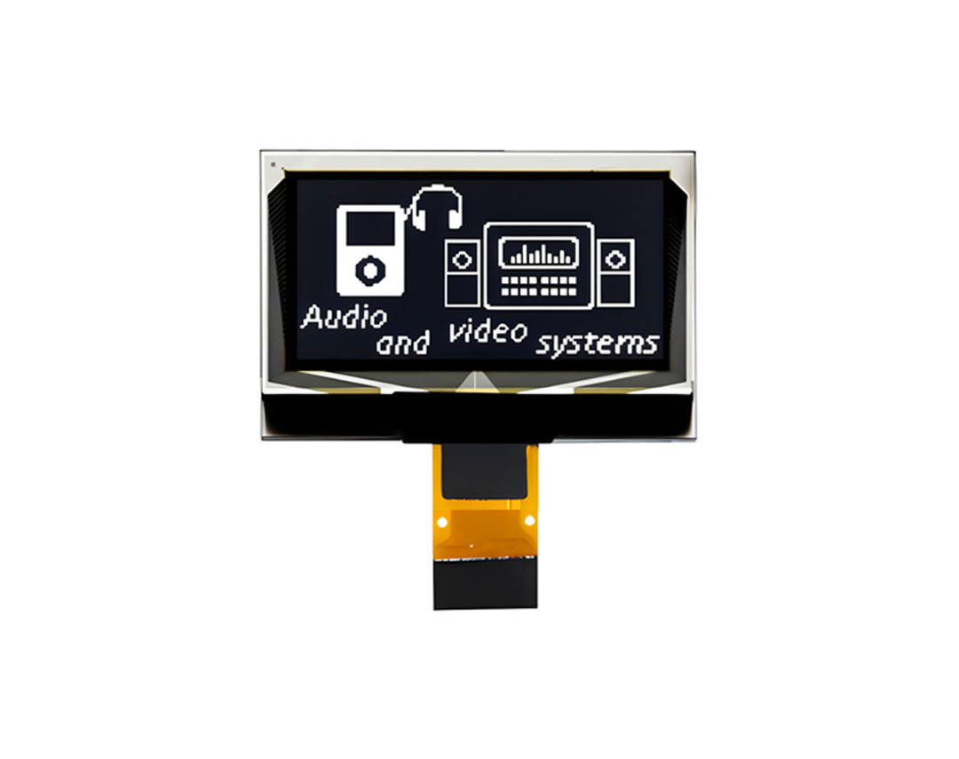
40mm ZIF FPC 1.12 英寸 OLED 显示屏产品图片


工厂设施及证书


手机/微信:135 0298 3321 柯先生
手机/微信:138 2960 7086 郑小姐
手机/微信:136 8686 7235 陈小姐
地址: 深圳市宝安区洲石路阳光工业区D栋


在线留言

 135 0298 3321
 首页 》
首页 》