TFT彩屏
TFT触摸屏
HDMI TFT显示器
工业级TFT屏
条型TFT屏
圆形TFT屏
方形TFT屏
全视角TFT屏
电阻触摸TFT屏
电子墨水屏
高亮液晶屏
树莓派触摸屏
OLED模块
TFT彩屏
TFT触摸屏
HDMI TFT显示器
工业级TFT屏
条型TFT屏
圆形TFT屏
方形TFT屏
全视角TFT屏
电阻触摸TFT屏
电子墨水屏
高亮液晶屏
树莓派触摸屏
OLED模块

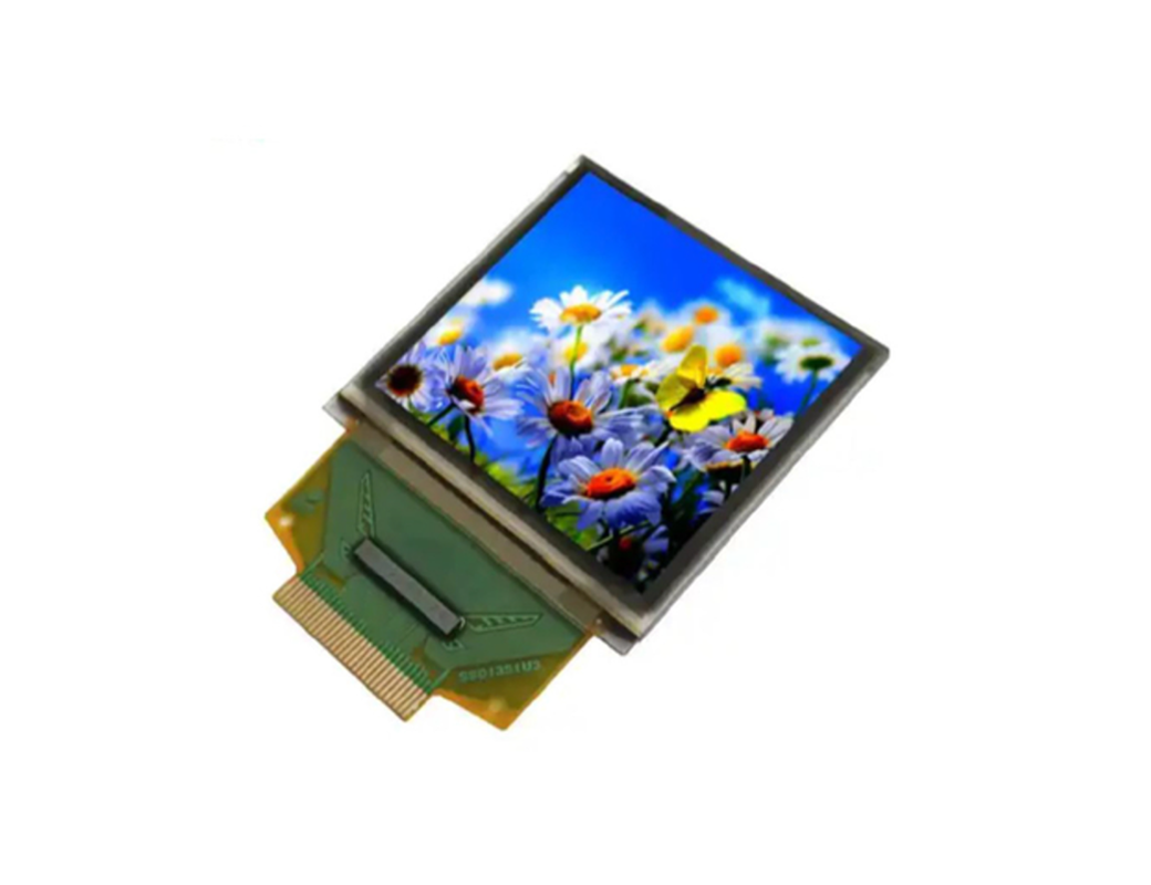
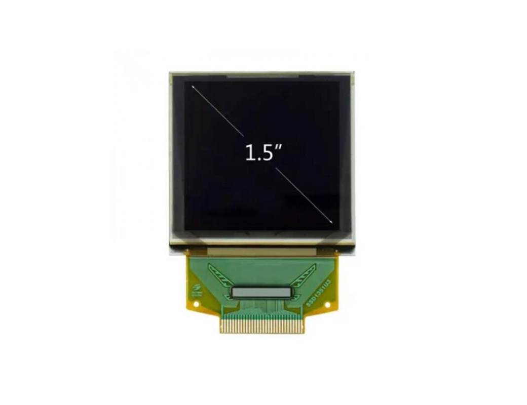
揭开尖端技术的面纱:1.5 英寸 AMOLED 显示屏,具有 128×128 像素和 262k 色彩亮度,采用 UG-2828GDEDF11 SSD1351 控制器
产品概述
借助我们最先进的有机发光二极管 (OLED) 技术迈向未来,提供无与伦比的亮度、清晰的图像和闪电般的响应时间。推出 UG-2828GDEDF11 OLED 显示屏,这是一款 1.5 英寸的奇迹,拥有 120 x 128 像素的鲜艳单色亮度。这款 OLED 模块具有轻盈的构造、最低功耗和紧凑的设计,提供一系列接口选项,包括默认 SPI、并行和 I2C 接口。
沉浸式体验,有效区域对角线长度为 1.5 英寸,封装尺寸为 33.80 × 34.00 × 1.60 (mm)。有效区域本身跨度为 26.855 × 26.864 (mm),为绚丽提供画布。这款 1.5 英寸 OLED 显示屏配备先进的 IC SSD1315,对比度高达 20,000:1。逻辑电源电压范围为 1.65V 至 3.5V,典型值为 3V。
应用
从医疗设备到 POS 系统、白色家电和家庭应用,拥抱各种应用的可能性。这款 OLED 显示屏适用于工业仪器、自动化、视听显示系统、个人护理电器、家居用品、汽车显示屏和动态信息显示屏。这款前卫显示屏将创新与卓越相结合,提升您的技术体验。
产品特点
| Product: | 1.5″ Inch Color AMOLED Display |
| Resolution: | 128×128 Pixels Resolution |
| Display Mode: | Passive Matrix |
| Interface: | 8-bit 68XX/80XX Parallel, 4-wire SPI, I2C |
| Display Color: | Full Color |
| Optics: | All Viewing Angles |
| Outline Dim.: | 33.80 × 34.00 × 1.60 (mm) |
| Active Area: | 26.855 × 26.864 (mm) |
| Pixel Pitch: | 0.07 × 0.21 (mm) |
| Operating Temp: | -40°C To +70°C |
| Storage Temp.: | -40°C To +85°C |
| Driver IC: | SSD1315 |
| Supply Voltage For Logic: | 1.65 – 3.5V |
| Pin Number: | 30 Pins |
| IC Package Type: | COF |
| Module Connecting Type: | ZIF |
| Duty: | 1/128 |
| Compliance: | REACH & RoHS Compliant |
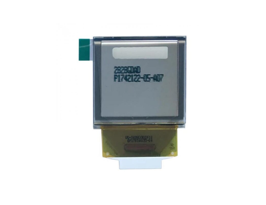
1.5 英寸 128×128 点 262k 色 SSD1351 AMOLED 显示屏产品图纸

接口管脚定义
| Pin Number | Symbol | Type | Function |
| Power Supply | |||
| 27 | VCI | P | Power Supplyfor Operation This is a voltage supply pin. It must be connected to external source & always be equal to or higher than VDD & VDDIO. |
| 26 | VDD | P | Power Supplyfor Core Logic Circuit This is a voltage supply pin which is regulated internally from VCI. A capacitor should be connected between this pin & VSS under all circumstances. |
| 4 | VDDIO | P | Power Supplyfor I/OPin This pin is a power supply pin of I/O buffer. It should be connected to VCI or external source. All I/O signal should have VIH reference to VDDIO. When I/O signal pins (BS0~BS1, D0~D7, control signals…) pull high, they should be connected to VDDIO. |
| 28 | VSS | P | Ground of OEL System This is a ground pin. It also acts as a reference for the logic pins, the OEL driving voltages, and the analog circuits. It must be connected to external ground. |
| 2 | VCC | P | Power Supplyfor OEL Panel This is the most positive voltage supply pin It must be connected to external source. of the chip |
| Driver | |||
| 22 | IREF | I | Current Referencefor Brightness Adjustment This pin is segment current reference pin. A resistor should be connected between this pin and VSS. Set the current lower than 12.5uA. |
| 3 | VCOMH | P | Voltage Ouut High Levelfor COM Signal This pin is the input pin for the voltage output high level for COM signals. A tantalum capacitor should be connected between this pin and VSS. |
| 5 | VSL | P | Voltage Ouut Low Levelfor SEG Signal This is segment voltage reference pin. When external VSL is not used, this pin should be left open. When external VSL is used, this pin should connect with resistor and diode to ground. |
| External IC Control | |||
| 24 23 | GPIO0 GPIO1 | I/O | General Purpose Input/Ouut These pins could be left open individually or have signal inputted/outputted. They are able to use as the external DC/DC converter circuit enabled/disabled control or other applications. |
| Interface | |||
| 17 18 | BS0 BS1 | I | Communicating Protocol Select These pins are MCU interface selection input.See the following table: BS0 BS1 3-wire SPI, 1, 0 4-wire SPI, 0, 0 68XX-parallel (8-bit), 1, 1 80XX-parallel (8-bit), 0, 1 |
| 21 | RES# | I | Power Reset for Controller and Driver This pin is reset signal input. When the pin is low, initialization of the chip is executed. |
| 19 | CS# | I | Chp Select This pin is the chip select input. The chip is enabled for MCU communication only when CS# is pulled low. |
| 20 | D/C# | I | Data/Command Control This pin is Data/Command control pin. When the pin is pulled high, the input at D7~D0 is treated as display data. When the pin is pulled low, the input at D7~D0 will be transferred to the command register. For detail relationship to MCU interface signals, please refer to the Timing Characteristics Diagrams. When 3-wire serial mode is selected, this pin must be connected to VSS. |
| 15 | E/RD# | I | Read/Write Enable or Read This pin is MCU interface input. When interfacing to a 68XX-series microprocessor, this pin will be used as the Enable (E) signal. Read/write operation is initiated when this pin is pulled high and the CS# is pulled low. When connecting to an 80XX-microprocessor, this pin receives the Read (RD#) signal. Data read operation is initiated when this pin is pulled low and CS# is pulled low. When serial mode is selected, this pin must be connected to VSS. |
| 16 | R/W# | I | Read/Write Select or Write This pin is MCU interface input. When interfacing to a 68XX-series microprocessor, this pin will be used as Read/Write (R/W#) selection input. Pull this pin to “High” for read mode and pull it to “Low” for write mode. When 80XX interface mode is selected, this pin will be the Write (WR#) input. Data write operation is initiated when this pin is pulled low and the CS# is pulled low. When serial mode is selected, this pin must be connected to VSS. |
| 7~14 | D7~D0 | I/O | Host Data Input/Ouut Bus These pins are 8-bit bi-directional data bus to be connected to the microprocessor’s data bus. When serial mode is selected, D1 will be the serial data input SDIN and D0 will be the serial clock input SCLK. Unused pins must be connected to VSS except for D2. |
| Reserve | |||
| 6, 25, 29 | N.C. | – | Reserved Pin The N.C. pins between function compatible and flexible design. pins are reserved |
| 1, 30 | N.C. (GND) | – | Reserved Pin (Supporting Pin) The supporting pins can reduce the influences from stresses on the function pins. These pins must be connected to external ground. |
1.5 英寸 128×128 像素 262k 色 SSD1351 AMOLED 显示屏 产品图片


手机/微信:135 0298 3321 柯先生
手机/微信:138 2960 7086 郑小姐
手机/微信:136 8686 7235 陈小姐
地址: 深圳市宝安区洲石路阳光工业区D栋


在线留言

 135 0298 3321
 首页 》
首页 》