TFT彩屏
TFT触摸屏
HDMI TFT显示器
工业级TFT屏
条型TFT屏
圆形TFT屏
方形TFT屏
全视角TFT屏
电阻触摸TFT屏
电子墨水屏
高亮液晶屏
树莓派触摸屏
OLED模块
TFT彩屏
TFT触摸屏
HDMI TFT显示器
工业级TFT屏
条型TFT屏
圆形TFT屏
方形TFT屏
全视角TFT屏
电阻触摸TFT屏
电子墨水屏
高亮液晶屏
树莓派触摸屏
OLED模块


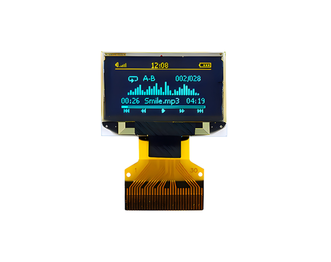
揭开尖端技术的面纱:3.12 英寸 OLED 显示模块,像素为 256×64
借助我们的 OLED 显示模块,踏入创新领域,该模块采用先进的 OLED 技术。3.12 英寸 OLED 显示模块,编号为 SFOS312YZ-7091AN,是更明亮、更清晰的图像以及敏捷响应速度的证明。
拥抱未来:
· OLED 模块由 256 x 64 个单色点组成,突破了视觉卓越的界限。
· 重量轻、功耗低、设计紧凑,提供各种可选接口,默认为 SPI、并行和 I2C 接口。
重要规格:
· 有效区域对角线跨度为 3.12 英寸,模块尺寸为 88.00(宽)x 27.80(高)毫米,有效区域尺寸为 76.78(宽)x 19.18(高)毫米。
· 这款 3.12 英寸 OLED 显示屏配备 SSD1322 IC,拥有令人印象深刻的 20,000:1 高对比度。
· 逻辑电源电压范围为 2.4V 至 2.6V(典型值:2.5V),可满足各种应用需求。
应用:
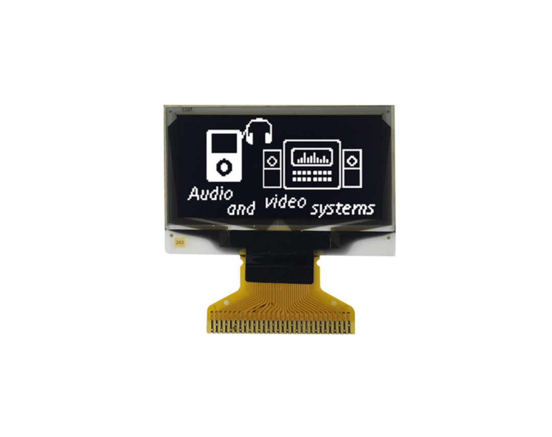
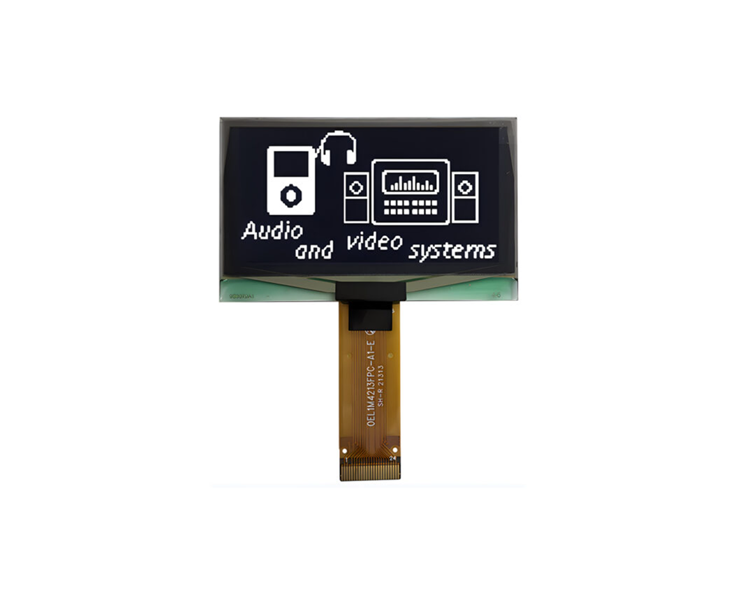
适用于各种应用,包括医疗设备、POS 系统、白色家电、家庭应用、工业仪器、自动化、音频/视频显示系统、个人护理用具、家居用品、汽车显示器和动态信息显示器。
产品特点:
| Product: | 3.12″ Inch Passive OLED |
| Resolution: | 256×64 Pixels Resolution |
| Display Mode: | Passive Matrix |
| Interface: | Parallel, SPI Optional |
| Display Color: | White, Yellow |
| Optics: | All Viewing Angles |
| Outline Dim.: | 88.00 (W) X27.80 (H) |
| Active Area: | 76.78 (W) X 19.18 (H) |
| Pixel Pitch: | 0.30 (W) X 0.30 (H) |
| Operating Temp: | -40°C To +80°C |
| Storage Temp.: | -40°C To +85°C |
| Driver IC: | SSD1322 |
| Supply Voltage: | 2.4 – 3.5V |
| Pin Number: | 30 Pins |
| Compliance: | REACH & RoHS Compliant |
| IC Package Type: | COF |
| Module Connecting Type: | ZIF |
| Duty: | 1/64 |
3.12 英寸 256×64 像素 OLED 显示屏 SSD1322 并行 SPI 接口图

接口 引脚 功能
| Pin Number | Symbol | I/O | Function |
| 1 | N.C. (GND) | P | Ground |
| 2 | VSS | P | Ground. |
| 3 | VCC | P | Power supply for panel driving voltage. This is also the most positive power voltage supply pin. |
| 4 | VCOMH | P | COM signal deselected voltage level. A capacitor should be connected between this pin and VSS. |
| 5 | VLSS | P | Analog system ground pin. |
| 6~13 | D7~D0 | I/O | Host Data Input/Output Bus These pins are 8-bit bi-directional data bus to be connected to the microprocessor’s data bus. When serial mode is selected, D1 will be the serial data input SDIN and D0 will be the serial clock input SCLK. |
| 14 | E/RD# | I | Read/Write Enable or Read This pin is MCU interface input. When interfacing to a 68XX-series microprocessor, this pin will be used as the Enable (E) signal. Read/write operation is initiated when this pin is pulled high and the CS# is pulled low. When connecting to an 80XX-microprocessor, this pin receives the Read (RD#) signal. Data read operation is initiated when this pin is pulled low and CS# is pulled low. When serial mode is selected, this pin must be connected to VSS. |
| 15 | R/W# | I | Read/Write Select or Write This pin is MCU interface input. When interfacing to a 68XX-series microprocessor, this pin will be used as Read/Write (R/W#) selection input. Pull this pin to “High” for read mode and pull it to “Low” for write mode. When 80XX interface mode is selected, this pin will be the Write (WR#) input. Data write operation is initiated when this pin is pulled low and the CS# is pulled low. When serial mode is selected, this pin must be connected to VSS. |
| 16 | BS0 | I | Communicating Protocol Select These pins are MCU interface selection input. See the following table: BS:[1:0] Bus Interface Selection 00 4 line SPI 01 3 line SPI 10 8-bit 8080 parallel 11 8-bit 6800 parallel Note (1) 0 is connected to VSS (2) 1 is connected to VDDIO |
| 17 | BS1 | ||
| 18 | D/C# | I | Data/Command Control This pin is Data/Command control pin connecting to the MCU. When the pin is pulled HIGH, the content at D[7:0] will be interpreted as data. When the pin is pulled LOW, the content at D[7:0] will be interpreted as command. |
| 19 | CS# | I | Data/Command Control This pin is the chip select input connecting to the MCU. The chip is enabled for MCU communication only when CS# is pulled LOW. |
| 20 | RES# | I | This pin is reset signal input. When the pin is pulled LOW, initialization of the chip is executed. Keep this pin pull HIGH during normal operation. |
| 21 | FR | O | This pin is No Connection pins. Nothing should be connected to this pin. This pin should be left open individually. |
| 22 | IREF | I | Current Reference for Brightness Adjustment This pin is segment current reference pin. A resistor should be connected between this pin and VSS. Set the current lower than 10uA. |
| 23 | N.C. | – | Reserved Pin The N.C. pin between function pins are reserved for compatible and flexible design. |
| 24 | VDDIO | P | Power Supply for I/O Pin It should be matched with the MCU interface voltage level. |
| 25 | VDD | P | Power Supply for Core Logic Circuit Power supply pin for core logic operation. A capacitor is required to connect between this pin and VSS |
| 26 | VCI | P | Power Supply for Operation VCI must always be equal to or higher than VDD and VDDIO. |
| 27 | VSL | P | Voltage Output Low Level for SEG Signal This is segment voltage reference pin. When external VSL is not used, this pin should be left open. When external VSL is used, this pin should connect with resistor and diode to ground. |
| 28 | VLSS | P | Ground of Analog Circuit These are the analog ground pins. They should be connected to VSS externally. |
| 29 | VCC | P | Power Supply for OLED Panel These are the most positive voltage supply pin of the chip. They must be connected to external source. |
| 30 | N.C. (GND) | P | Ground |
3.12 英寸 256×64 像素 OLED 显示屏 SSD1322 并行 SPI 接口图像


手机/微信:135 0298 3321 柯先生
手机/微信:138 2960 7086 郑小姐
手机/微信:136 8686 7235 陈小姐
地址: 深圳市宝安区洲石路阳光工业区D栋


在线留言

 135 0298 3321
 首页 》
首页 》