TFT彩屏
TFT触摸屏
HDMI TFT显示器
工业级TFT屏
条型TFT屏
圆形TFT屏
方形TFT屏
全视角TFT屏
电阻触摸TFT屏
电子墨水屏
高亮液晶屏
树莓派触摸屏
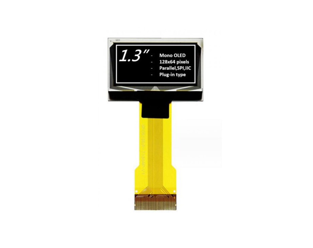
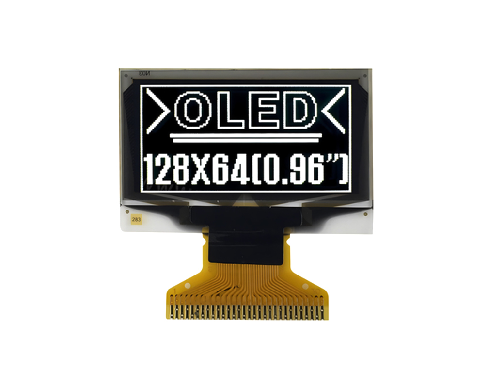
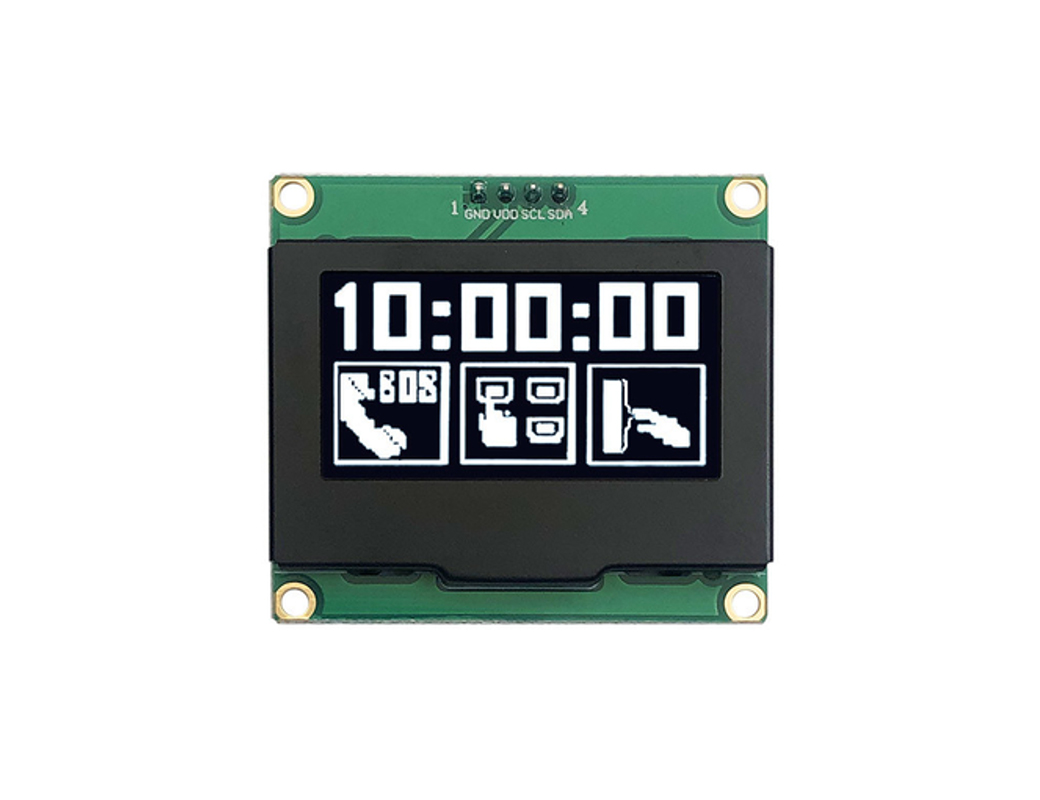
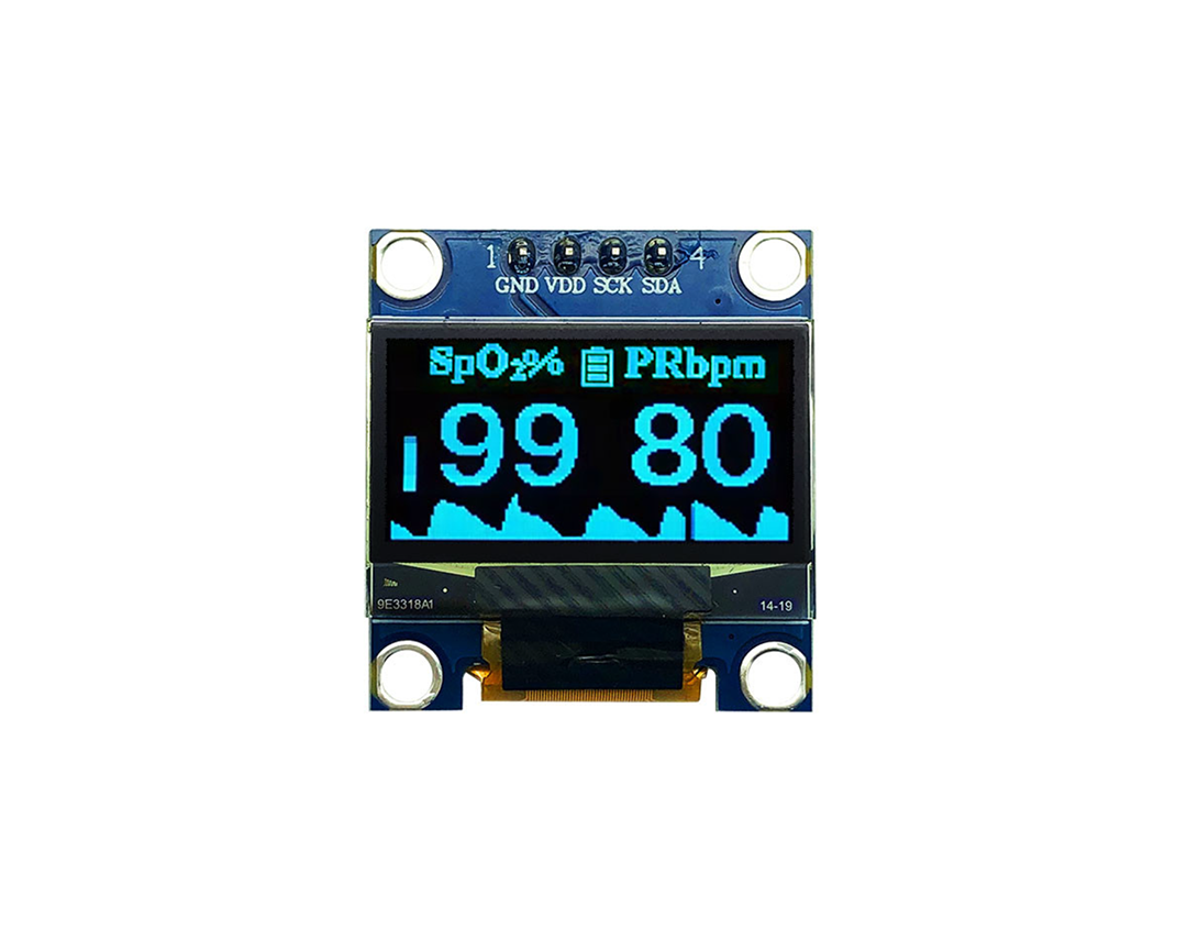
OLED模块
TFT彩屏
TFT触摸屏
HDMI TFT显示器
工业级TFT屏
条型TFT屏
圆形TFT屏
方形TFT屏
全视角TFT屏
电阻触摸TFT屏
电子墨水屏
高亮液晶屏
树莓派触摸屏
OLED模块

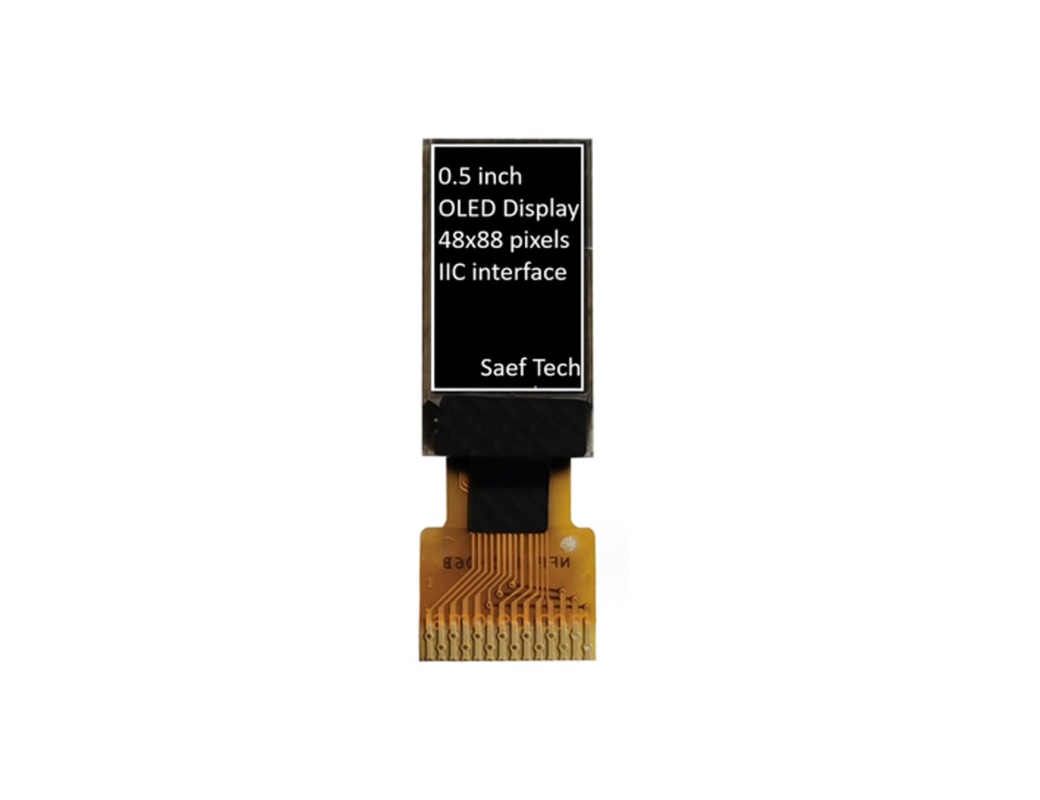
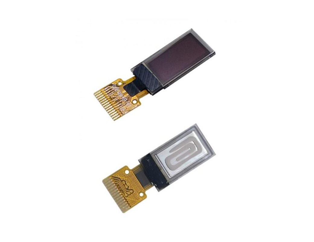
揭开创新面纱:分辨率为 88×48 的 0.5 英寸 OLED 显示模块
SFOS050XZ-7112AN OLED 显示模块让您迈向未来,该模块拥有令人印象深刻的 88×48 分辨率,对角线尺寸仅为 0.5 英寸。这款 COG 图形显示器不仅令人惊叹,而且是一款工业级强大产品,将尖端功能与具有竞争力的价格相结合。该模块嵌入了先进的 CH1115 IC 并支持多功能 I2C 接口,为显示技术树立了新标准。
供电可能性:主要规格
· 逻辑电源电压:2.8V
· 显示电源电压:9V
· VDD 工作电流:180μA
· 驱动占空比:1/48
SFOS50XZ-7112AN OEL显示模块不受产品应用环境限制,是可穿戴设备、智能家居应用等领域的首选解决方案。该模块可在-40℃至+80℃的温度范围内无缝运行,并具有-40℃至+85℃的存储容量,确保在任何环境下的可靠性。
| Product: | 0.5 Inch OLED Display Module |
| Number Of Pixels: | 48×88 Pixels |
| Driver IC: | CH1115 Or Equivalent |
| Display Mode: | Passive Matrix |
| Display Color: | Monochrome (white) |
| Drive Duty: | 1/48 Duty |
| Panel Size: | 8.928 X 17.1 X 1.227 (mm) |
| Active Area: | 6.124 X 11.244 (mm) |
| Pixel Pitch: | 0.128 X 0.128 (mm) |
| Pixel Size: | 0.108 X 0.108 (mm) |
| Viewing Direction: | All Viewing Angles |
| Interface: | I2C |
| Connection: | Soldering/Hotbar (customizable) |
| Pin Number: | 14 Pins |
| Life Time: | 50,000 Hours @60cd/m2 |
| Compliance: | REACH & RoHS Compliant |
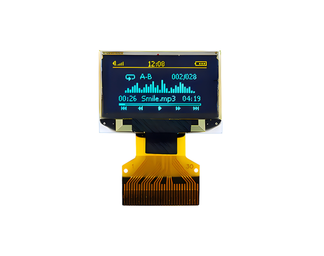
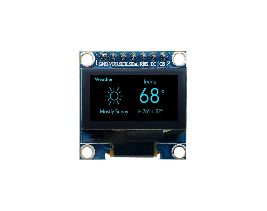
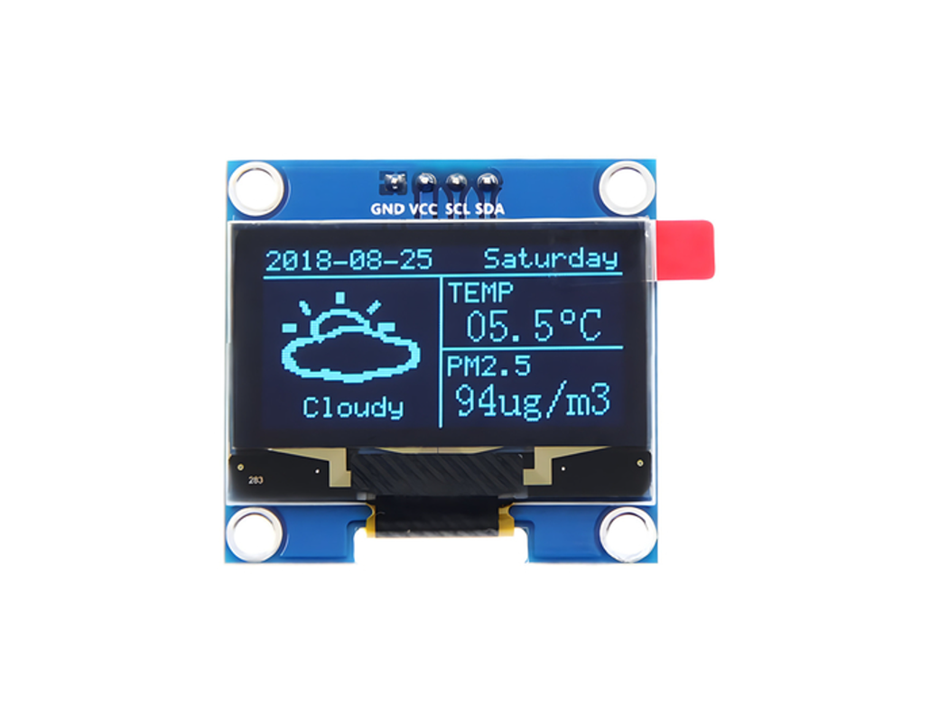
88×48像素矩阵0.5英寸OLED显示模块产品图纸

引脚定义
Pin1, C2P / Pin2, C2N / Pin3, C1P / Pin4, C1N
Positive Terminal of the Flying Inverting Capacitor, Negative Terminal of the Flying Boost Capacitor. The charge-pump capacitors are required between the terminals. They must be floated when the converter is not used.
Pin5, VDD2 VBAT
Power Supply for DC/DC Converter Circuit. This is the power supply pin for the internal buffer of the DC/DC voltage converter. It must be connected to external source when the converter is used. It should be connected to VDD when the converter is not used.
Pin6, VBREF NC
Pin7, VSS
Ground of Logic Circuit. This is a ground pin. It acts as a reference for the logic pins. It must be connected to external ground.
Pin8, VDD1
Power Supply for Logic. This is a voltage supply pin. It must be connected to external source.
Pin9, RES#
Power Reset for Controller and Driver. This pin is reset signal input. When the pin is low, initialization of the chip is executed. Keep this pin pull high during normal operation.
Pin10, SCL
IIC Bus Clock Signal. The transmission if information in the I2C bus is following a clock signal. Each transmission of data bit is taken place during a single clock period of this pin.
Pin11, SDA
I2C Bus Data Signal. This pin acts as a communication channel between the transmitter and the receiver.
Pin12, IREF
Current Reference for Brightness Adjustment. This pin is a segment current reference pin. A resistor should be connected between this pin and VSS. Set the current at 12.5uA maximum.
Pin13, VCOMH
Voltage Output High Level for COM Signal. This pin is the input pin for the voltage output high level for COM signals. A capacitor should be connected between this pin and VSS.
Pin14, VCC
Power Supply for OEL Panel. This is the most positive voltage supply pin of the chip. A stabilization capacitor should be connected between this pin and VSS when the converter is used. It must be connected to external source when the converter is not used.

注 1:以上所有电压均以“VSS = 0V”为基准。
注 2:当此模块的使用超出上述绝对最大额定值时,可能会发生模块永久性损坏。此外,为了正常运行,最好在第 3 节“光学和电气特性”的条件下使用此模块。如果超出这些条件使用此模块,可能会发生模块故障,并且模块的可靠性可能会下降。
注 3:定义的温度范围不包括偏振器。偏振器的最大耐受温度应为 80°C。
注 4:VPP = 7.5V,Ta = 25°C,50% 棋盘。软件配置遵循第 4.4 节初始化。寿命结束规定为达到初始亮度的 50%。室温下的平均工作寿命是通过高温条件下的加速操作估算的。

88×48像素矩阵0.5英寸OLED显示模块产品图片


手机/微信:135 0298 3321 柯先生
手机/微信:138 2960 7086 郑小姐
手机/微信:136 8686 7235 陈小姐
地址: 深圳市宝安区洲石路阳光工业区D栋


在线留言

 135 0298 3321
 首页 》
首页 》