TFT彩屏
TFT触摸屏
HDMI TFT显示器
工业级TFT屏
条型TFT屏
圆形TFT屏
方形TFT屏
全视角TFT屏
电阻触摸TFT屏
电子墨水屏
高亮液晶屏
树莓派触摸屏
OLED模块
TFT彩屏
TFT触摸屏
HDMI TFT显示器
工业级TFT屏
条型TFT屏
圆形TFT屏
方形TFT屏
全视角TFT屏
电阻触摸TFT屏
电子墨水屏
高亮液晶屏
树莓派触摸屏
OLED模块

产品概述
产品快速概览:
· 型号 SF-TO700GLTB-8976A-CT
· 尺寸:7 英寸
· 分辨率:1024 x 600 点
· 接口:MIPI
· 视角:IPS,全视角
· 亮度 (cd/m²):500,(300nits、1000nits 可选)
· 触摸屏:投射电容式触摸屏 (PCAP)
· 检测点:5 根手指
产品描述:
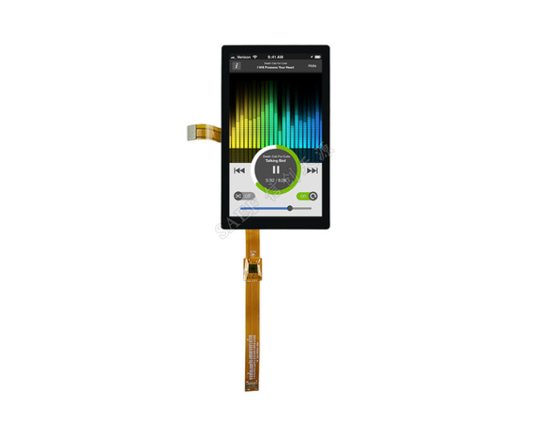
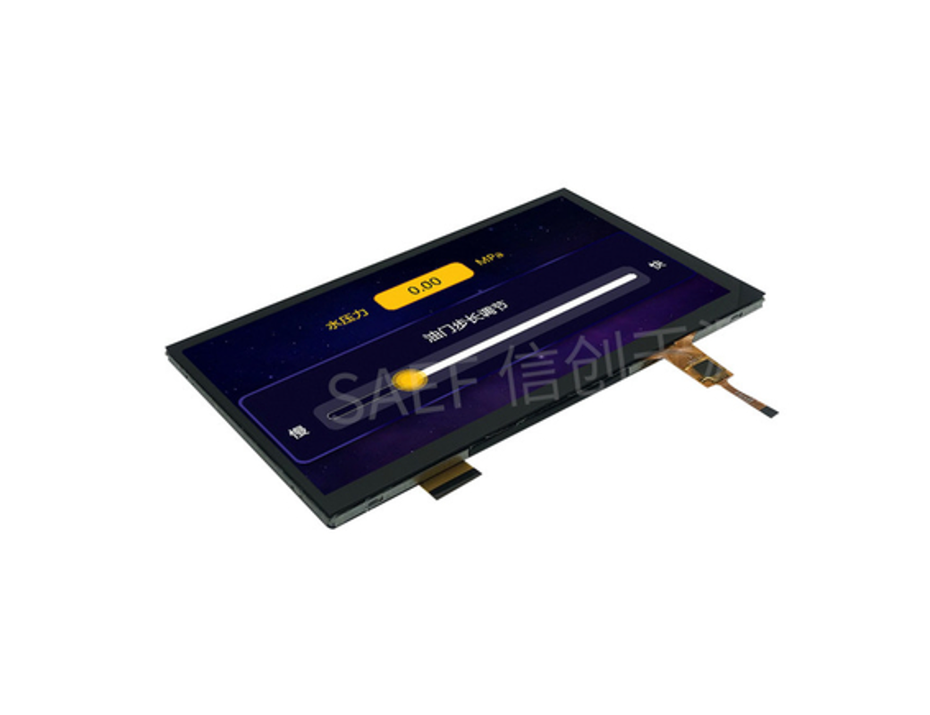
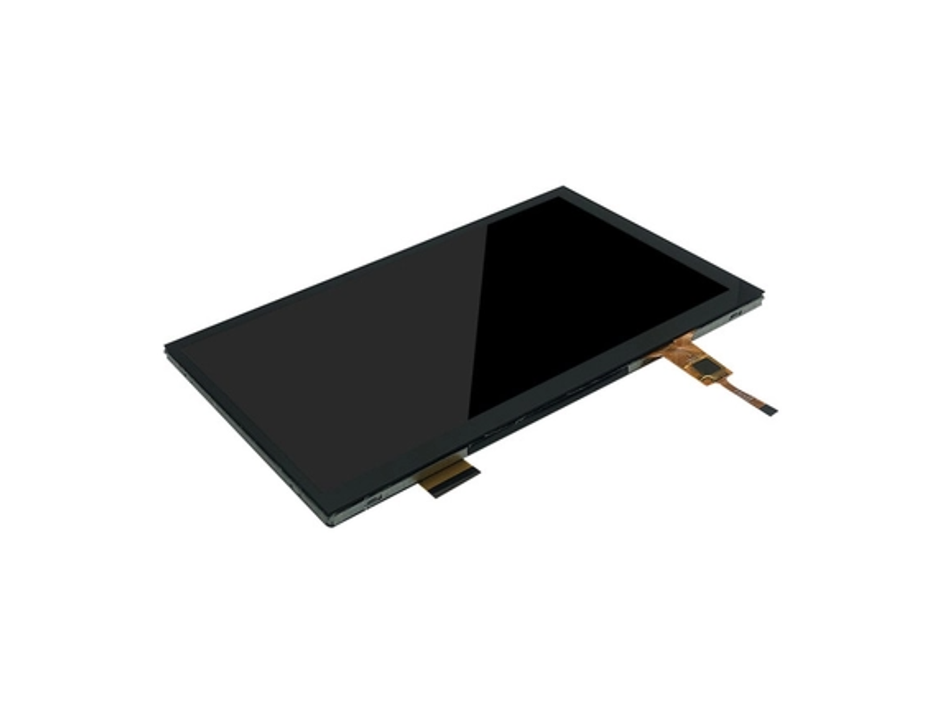
1、SF-TO700GLTB-8976A-CT是一款7英寸IPS全视角TFT LCD显示屏,分辨率为1024×600像素。它带有电容式触摸屏(CTP),盖板玻璃可定制。
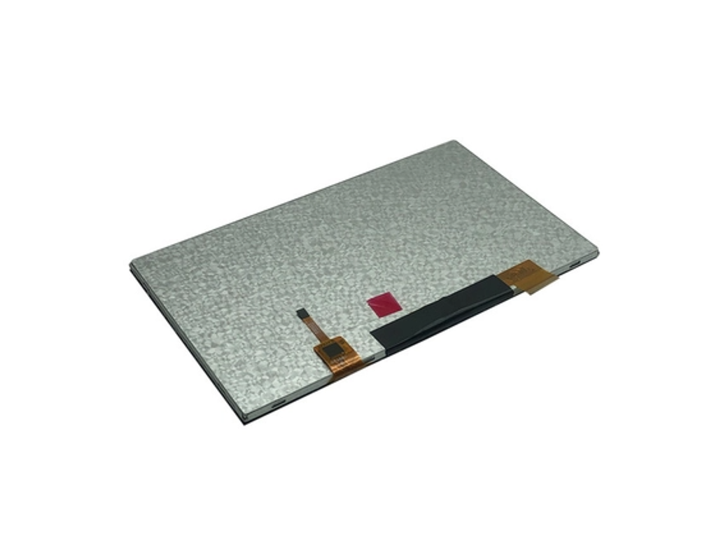
2、SF-TO700GLTB-8976A-CT TFT LCD模块的外形尺寸为164.7*99*2.6毫米,AA尺寸为154.21×85.92毫米。
3、SF-TO700GLTB-8976A-CT LCM接口为MIPI接口,30针。CTP接口为I2C。
4、SF-TO700GLTB-8976A-CT触摸屏表面亮度为500cd/m2(尼特),也可设计为1000cd/m2(尼特)。详情请联系我们的销售人员。
5、这款7英寸TFT LCD模块广泛应用于测量设备、医疗设备、家庭自动化、门禁安全系统、超市价格标签、家用电器、GPS设备等。
规格参数
| Product: | 7″ Inch PCAP Touch Screen |
| TFT Interface: | MIPI |
| Surface Luminance: | 500 Cd/m2 |
| Cover Glass Dimension: | Customizable |
| Viewing Direction: | IPS All Viewing Angle (80/80/80/80) |
| Operating Temp.: | –20℃ To +70℃ |
| Resolution: | 1024×600 |
| CTP Interface: | I2C Interface |
| Touch Screen: | CTP (Capacitive Touch Screen) |
| Pins: | 30 |
| LED Lifetime: | 40,000 Hours |
| Compliance: | REACH & RoHS Compliant |
外形结构图


接口引脚定义
| Pin No. | Symbol | Function |
| 1 | VLED+ | LED Anode |
| 2 | VLED+ | LED Anode |
| 3 | VGH | Positive power for TFT |
| 4 | VGL | Negative power for TFT |
| 5 | UPDN | Gate up or down scan control. UPDN = ”L”, STV2 output vertical start pulse and UD pin output logical “L” to Gate driver. (default) UPDN = ”H”, STV1 output vertical start pulse and UD pin output logical “H” to Gate driver |
| 6 | SHLR | Source right or left sequence control. SHLR = ”L“, shift left: last data = S1←S2←S3……….←S1536 = first data. SHLR = ”H“, shift right: first data = S1→S2→S3……..→S1536 = last data.(default) |
| 7 | VLED- | LED Cathode |
| 8 | VLED- | LED Cathode |
| 9 | AVDD | Power for Analog Circuit |
| 10 | GND | Ground |
| 11 | D3P | MIPI data input. |
| 12 | D3N | MIPI data input. |
| 13 | GND | Ground |
| 14 | D2P | MIPI data input. |
| 15 | D2N | MIPI data input. |
| 16 | GND | Ground |
| 17 | CLKP | MIPI clock input |
| 18 | CLKN | MIPI clock input |
| 19 | GND | Ground |
| 20 | D1P | MIPI data input. |
| 21 | D1N | MIPI data input. |
| 22 | GND | Ground |
| 23 | D0P | MIPI data input. |
| 24 | D0N | MIPI data input. |
| 25 | GND | Ground |
| 26 | STBYB | Standby mode. STBYB = ”H“, normal operation(default) STBYB = ”L”, timing controller, source driver will turn off, all output are GND. |
| 27 | RESET | Global reset pin. Active Low to enter Reset State. Normally pull high. Connecting with an RC reset circuit for stability. |
| 28 | VDD(1.8V) | Digital circuit |
| 29 | VDD(1.8V) | Digital circuit |
| 30 | VCOMIN | Common voltage |
直流特性 (VDD=2.8V,Ta=25°C)
| Item | Symbol | Min | Type | Max | Unit | Test condition |
| Operating voltage | VDD | 2.6 | 2.8 | 3.3 | V | – |
| Supply current | IDD | – | – | 5 | mA | VDD=2.8V,Ta=25°C |
| Input voltage | VIH | 0.8VDD | – | VDD | V | – |
| VIL | 0 | – | 0.2VDD | V | ||
| Input leakage current | IIL | -1.0 | – | 1.0 | mA | VIN=VDD or VSS |
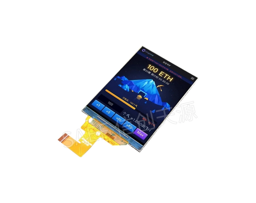
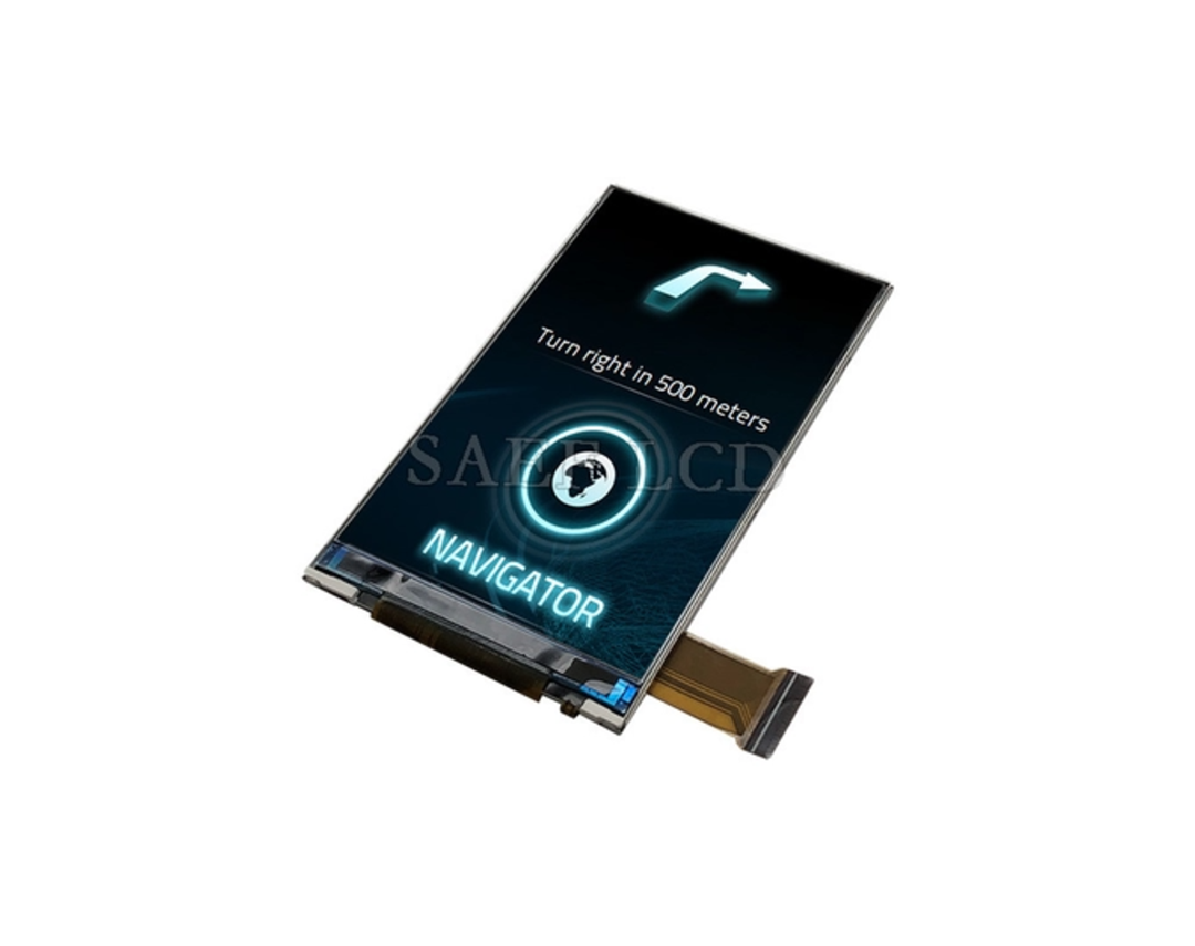
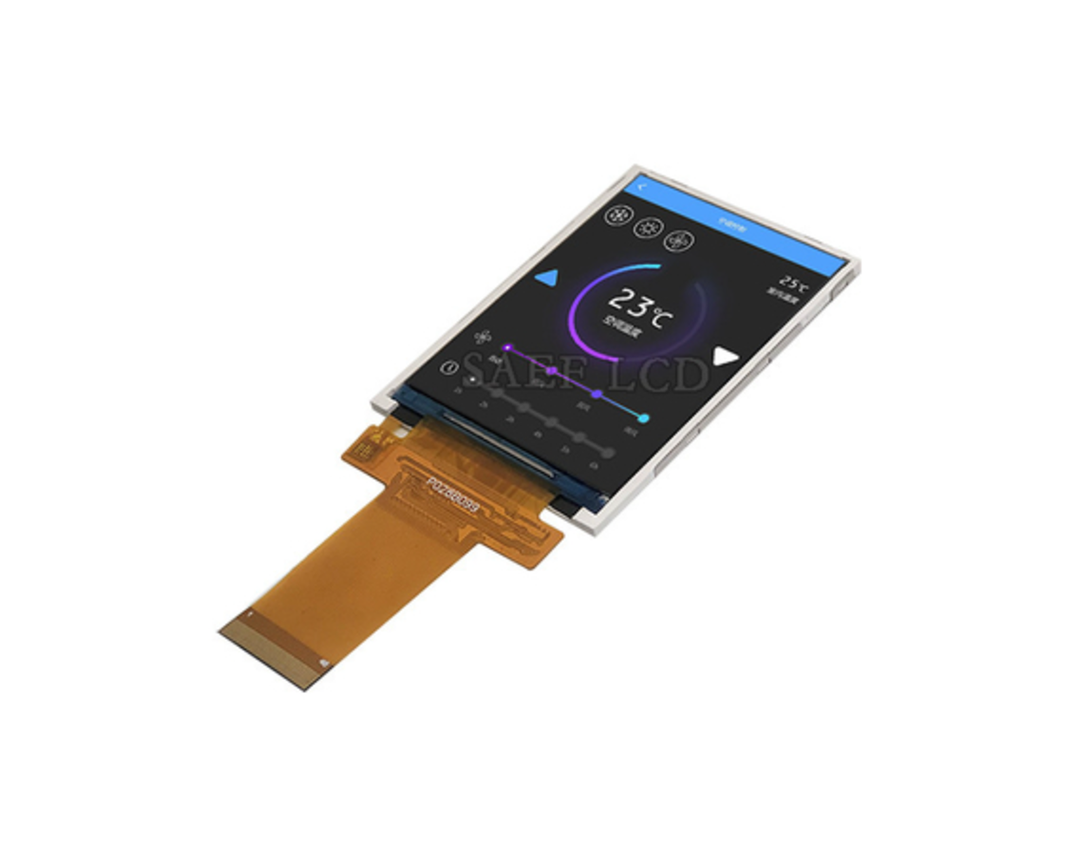
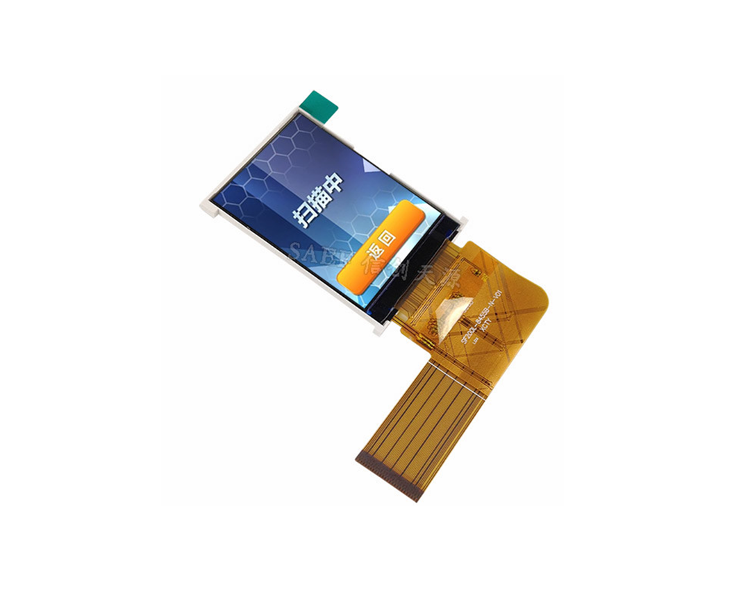
产品图片


手机/微信:135 0298 3321 柯先生
手机/微信:138 2960 7086 郑小姐
手机/微信:136 8686 7235 陈小姐
地址: 深圳市宝安区洲石路阳光工业区D栋


在线留言

 135 0298 3321
 首页 》
首页 》